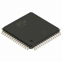
CY7C4225-15AC Cypress Semiconductor Corp, CY7C4225-15AC Datasheet - Page 9

CY7C4225-15AC
Manufacturer Part Number
CY7C4225-15AC
Description
IC SYNC FIFO MEM 1KX18 64LQFP
Manufacturer
Cypress Semiconductor Corp
Series
CY7Cr
Specifications of CY7C4225-15AC
Function
Synchronous
Memory Size
18K (1K x 18)
Data Rate
100MHz
Access Time
10ns
Voltage - Supply
3.3V
Operating Temperature
-40°C ~ 85°C
Mounting Type
Surface Mount
Package / Case
64-LQFP
Configuration
Dual
Density
18Kb
Access Time (max)
10ns
Word Size
18b
Organization
1Kx18
Sync/async
Synchronous
Expandable
Yes
Bus Direction
Uni-Directional
Package Type
TQFP
Clock Freq (max)
66.7MHz
Operating Supply Voltage (typ)
5V
Operating Supply Voltage (min)
4.5V
Operating Supply Voltage (max)
5.5V
Supply Current
45mA
Operating Temp Range
0C to 70C
Operating Temperature Classification
Commercial
Mounting
Surface Mount
Pin Count
64
Lead Free Status / RoHS Status
Contains lead / RoHS non-compliant
Other names
428-1217
Available stocks
Company
Part Number
Manufacturer
Quantity
Price
Company:
Part Number:
CY7C4225-15AC
Manufacturer:
CYPRESS
Quantity:
13 888
Company:
Part Number:
CY7C4225-15AC
Manufacturer:
Cypress Semiconductor Corp
Quantity:
10 000
Document #: 38-06029 Rev. *C
AC Test Loads and Waveforms
Switching Characteristics
Equivalent to:
t
t
t
t
t
t
t
t
t
t
t
t
t
t
t
t
t
t
t
t
t
t
t
t
Notes:
10. C
11. Pulse widths less than minimum values are not allowed.
12. Values guaranteed by design, not currently tested.
13. t
S
A
CLK
CLKH
CLKL
DS
DH
ENS
ENH
RS
RSR
RSF
PRT
RTR
OLZ
OE
OHZ
WFF
REF
PAFasynch
PAFsynch
PAEasynch
PAEsynch
HF
9. C
Parameter
PAFasynch
L
L
= 30 pF for all AC parameters except for t
= 5 pF for t
, t
PAEasynch
OHZ
OUTPUT
Clock Cycle Frequency
Data Access Time
Clock Cycle Time
Clock HIGH Time
Clock LOW Time.
Data Set-up Time
Data Hold Time
Enable Set-up Time
Enable Hold Time
Reset Pulse Width
Reset Recovery Time
Reset to Flag and Output Time
Retransmit Pulse Width
Retransmit Recovery Time
Output Enable to Output in Low Z
Output Enable to Output Valid
Output Enable to Output in High Z
Write Clock to Full Flag
Read Clock to Empty Flag
Clock to Programmable Almost-Full Flag
Clock to Programmable Almost-Full Flag
Clock to Programmable Almost-Empty Flag
Clock to Programmable Almost-Full Flag
Clock to Half-Full Flag
OUTPUT
(Asynchronous mode, V
(Asynchronous mode, V
(Synchronous mode, V
(Synchronous mode, V
THÉVENIN EQUIVALENT
.
, after program register write will not be valid until 5 ns + t
3.3V
INCLUDING
JIG AND
SCOPE
C
L
Rth = 200Ω
R1 = 330Ω
[11]
Over the Operating Range
Description
CC
CC
CC
OHZ
[9, 10]
CC
/SMODE tied to V
/SMODE tied to V
/SMODE tied to V
R2 = 510Ω
/SMODE tied to V
.
Vth = 2.0V
[12]
[12]
[13]
CC
[13]
)
SS
SS
CC
)
)
)
PAF(E)
.
GND
3.0V
7C42X5V-15
Min.
≤ 3 ns
15
15
10
15
15
2
6
6
4
1
4
1
0
3
3
Max.
66.7
18
18
18
16
11
11
11
11
11
8
8
CY7C4225V/4205V/4215V
CY7C4425V/4235V/4245V
ALL INPUT PULSES
10%
90%
7C42X5V-25
Min.
25
10
10
25
15
25
25
2
6
2
6
2
0
3
3
Max.
40
15
25
12
12
15
15
22
15
22
15
20
7C42X5V-35
Min.
90%
35
14
14
35
20
35
35
2
7
2
7
2
0
3
3
10%
≤ 3 ns
Max.
28.6
Page 9 of 20
20
35
15
15
20
20
25
20
25
20
25
MHz
Unit
ns
ns
ns
ns
ns
ns
ns
ns
ns
ns
ns
ns
ns
ns
ns
ns
ns
ns
ns
ns
ns
ns
ns
[+] Feedback


