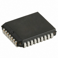
CY7C4251-15JXC Cypress Semiconductor Corp, CY7C4251-15JXC Datasheet - Page 10

CY7C4251-15JXC
Manufacturer Part Number
CY7C4251-15JXC
Description
IC SYNC FIFO MEM 8KX9 32-PLCC
Manufacturer
Cypress Semiconductor Corp
Series
CY7Cr
Specifications of CY7C4251-15JXC
Function
Synchronous
Memory Size
72K (8K x 9)
Data Rate
100MHz
Access Time
10ns
Voltage - Supply
3.3V
Operating Temperature
-40°C ~ 85°C
Mounting Type
Surface Mount
Package / Case
32-PLCC
Configuration
Dual
Density
64Kb
Access Time (max)
15ns
Word Size
9b
Organization
8Kx9
Sync/async
Synchronous
Expandable
Yes
Bus Direction
Uni-Directional
Clock Freq (max)
40MHz
Operating Supply Voltage (typ)
5V
Operating Supply Voltage (min)
4.5V
Operating Supply Voltage (max)
5.5V
Supply Current
35mA
Operating Temp Range
0C to 70C
Operating Temperature Classification
Commercial
Mounting
Surface Mount
Pin Count
32
Lead Free Status / RoHS Status
Lead free / RoHS Compliant
Available stocks
Company
Part Number
Manufacturer
Quantity
Price
Company:
Part Number:
CY7C4251-15JXC
Manufacturer:
ONSEMI
Quantity:
5 469
Company:
Part Number:
CY7C4251-15JXC
Manufacturer:
Cypress Semiconductor Corp
Quantity:
10 000
Company:
Part Number:
CY7C4251-15JXCT
Manufacturer:
Cypress Semiconductor Corp
Quantity:
10 000
Document #: 38-06016 Rev. *B
Switching Waveforms
Notes:
First Data Word Latency after Reset with Simultaneous Read and Write
Empty Flag Timing
17. The clocks (RCLK, WCLK) can be free-running during reset.
18. Holding WEN2/LD HIGH during reset will make the pin act as a second enable pin. Holding WEN2/LD LOW during reset will make the pin act as a load enable
19. After reset, the outputs will be LOW if OE = 0 and three-state if OE=1.
20. When t
21. The first word is available the cycle after EF goes HIGH, always.
(if applicable)
WEN2
Q
for the programmable flag offset registers.
t
D
CLK
WEN1
REN1,
WCLK
REN2
0
RCLK
0
–Q
–D
OE
+ t
EF
SKEW1
8
SKEW1
8
(if applicable)
D
LOW
Q
WEN2
WCLK
WEN1
REN1,
t
. The Latency Timing applies only at the Empty Boundary (EF = LOW).
RCLK
> minimum specification, t
REN2
DS
0
0
–D
–Q
OE
EF
t
t
ENS
ENS
8
8
DATAWRITE1
t
ENS
t
DS
(continued)
t
SKEW1
DATA IN OUTPUT REGISTER
t
ENH
t
ENH
D
0 (FIRST
t
FRL
FRL
(maximum) = t
[20]
VALID
t
SKEW1
Write)
t
OLZ
t
FRL
t
REF
CLK
[20]
+ t
SKEW1
t
D
REF
1
. When t
t
OE
t
SKEW1
A
t
REF
< minimum specification, t
t
DS
t
A
D
[21]
2
t
t
ENS
ENS
CY7C4421/4201/4211/4221
DATAWRITE2
t
ENH
t
SKEW1
t
ENH
CY7C4231/4241/4251
D
0
FRL
D
t
A
t
3
FRL
(maximum) = either 2*t
DATA Read
[20]
D
1
D
t
4
REF
Page 10 of 18
CLK
+ t
SKEW1
or


