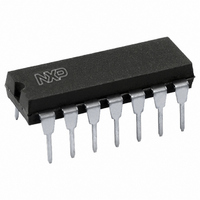
74HCT74N,652 NXP Semiconductors, 74HCT74N,652 Datasheet - Page 12

74HCT74N,652
Manufacturer Part Number
74HCT74N,652
Description
IC FLIP FLOP DUAL D TYPE 14DIP
Manufacturer
NXP Semiconductors
Series
74HCTr
Type
D-Typer
Datasheet
1.74HC74BQ115.pdf
(22 pages)
Specifications of 74HCT74N,652
Package / Case
14-DIP (0.300", 7.62mm)
Function
Set(Preset) and Reset
Output Type
Differential
Number Of Elements
2
Number Of Bits Per Element
1
Frequency - Clock
18MHz
Delay Time - Propagation
18ns
Trigger Type
Positive Edge
Current - Output High, Low
4mA, 4mA
Voltage - Supply
4.5 V ~ 5.5 V
Operating Temperature
-40°C ~ 125°C
Mounting Type
Through Hole
Number Of Circuits
2
Logic Family
74HCT
Logic Type
D-Type Flip-Flop
Polarity
Inverting/Non-Inverting
Input Type
Single-Ended
Propagation Delay Time
18 ns
High Level Output Current
- 4 mA
Supply Voltage (max)
5.5 V
Maximum Operating Temperature
+ 125 C
Mounting Style
SMD/SMT
Minimum Operating Temperature
- 40 C
Supply Voltage (min)
4.5 V
Technology
CMOS
Number Of Bits
2
Number Of Elements
2
Clock-edge Trigger Type
Positive-Edge
Operating Supply Voltage (typ)
5V
Package Type
PDIP
Low Level Output Current
4mA
Frequency (max)
18MHz
Operating Supply Voltage (min)
4.5V
Operating Supply Voltage (max)
5.5V
Operating Temp Range
-40C to 125C
Operating Temperature Classification
Automotive
Mounting
Through Hole
Pin Count
14
Lead Free Status / RoHS Status
Lead free / RoHS Compliant
Lead Free Status / RoHS Status
Lead free / RoHS Compliant, Lead free / RoHS Compliant
Other names
568-1566-5
74HCT74N
933669250652
74HCT74N
933669250652
Philips Semiconductors
Family 74HCT
GND = 0 V; t
2003 Jul 10
T
t
t
t
t
t
t
f
T
t
t
t
t
t
t
f
PHL
THL
W
rem
su
h
max
PHL
THL
W
rem
su
h
max
amb
amb
Dual D-type flip-flop with set and reset;
positive-edge trigger
SYMBOL
/t
/t
/t
/t
TLH
TLH
PLH
PLH
= 40 to +85 C
= 40 to +125 C
r
= t
propagation
delay nCP to nQ, nQ
propagation
delay nSD to nQ, nQ
propagation
delay nRD to nQ, nQ
output transition time
clock pulse width HIGH
or LOW
set or reset pulse width
LOW
removal time set or
reset
set-up time nD to nCP
hold time nCP to nD
maximum clock pulse
frequency
propagation
delay nCP to nQ, nQ
propagation
delay nSD to nQ, nQ
propagation
delay nRD to nQ, nQ
output transition time
clock pulse width HIGH
or LOW
set or reset pulse width
LOW
removal time set or
reset
set-up time nD to nCP
hold time nCP to nD
maximum clock pulse
frequency
f
= 6 ns; C
PARAMETER
L
= 50 pF.
see Fig.7
see Fig.8
see Fig.8
see Fig.7
see Fig.7
see Fig.8
see Fig.8
see Fig.7
see Fig.7
see Fig.7
see Fig.7
see Fig.8
see Fig.8
see Fig.7
see Fig.7
see Fig.8
see Fig.8
see Fig.7
see Fig.7
see Fig.7
WAVEFORMS
TEST CONDITIONS
12
4.5
4.5
4.5
4.5
4.5
4.5
4.5
4.5
4.5
4.5
4.5
4.5
4.5
4.5
4.5
4.5
4.5
4.5
4.5
4.5
V
CC
(V)
23
20
8
15
+3
22
27
24
9
18
3
18
MIN.
74HC74; 74HCT74
18
23
24
7
9
9
1
5
54
3
TYP.
Product specification
44
50
50
19
53
60
60
22
MAX.
ns
ns
ns
ns
ns
ns
ns
ns
ns
MHz
ns
ns
ns
ns
ns
ns
ns
ns
ns
MHz
UNIT


