IDT728980J IDT, Integrated Device Technology Inc, IDT728980J Datasheet
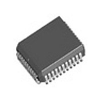
IC DGTL SW 256X256 44-PLCC

IDT728980J

Manufacturer Part Number
IDT728980J
Description
IC DGTL SW 256X256 44-PLCC
Manufacturer
IDT, Integrated Device Technology Inc
Series
7200r
Type
Multiplexerr
Datasheet

Specifications of IDT728980J

Circuit
1 x 8:8
Independent Circuits
1
Voltage Supply Source
Single Supply
Voltage - Supply
4.75 V ~ 5.25 V
Operating Temperature
-40°C ~ 85°C
Mounting Type
Surface Mount
Package / Case
44-PLCC
Lead Free Status / RoHS Status
Contains lead / RoHS non-compliant
Current - Output High, Low
-
Lead Free Status / RoHS Status
Not Compliant, Contains lead / RoHS non-compliant
Other names
728980J

Available stocks

Company
Part Number
Manufacturer
Quantity
Price
Part Number:
IDT728980J
Manufacturer:
IDT, Integrated Device Technology Inc
Quantity:
10 000
Part Number:
IDT728980J8
Manufacturer:
IDT, Integrated Device Technology Inc
Quantity:
10 000
Part Number:
IDT728980JG
Manufacturer:
IDT, Integrated Device Technology Inc
Quantity:
10 000
Part Number:
IDT728980JG
Manufacturer:
APTIX
Quantity:
7
Part Number:
IDT728980JG8
Manufacturer:
IDT, Integrated Device Technology Inc
Quantity:
10 000
microprocessor. The IDT728980 can handle as many as 256, 64 Kbit/s input
and output channels. Those 256 channels are divided into 8 serial inputs and
RX0
RX1
RX2
RX3
RX4
RX5
RX6
RX7
2001 Integrated Device Technology, Inc.
The IDT728980 is a ST-BUS
256 x 256 channel non-blocking switch
Serial Telecom Bus Compatible (ST-BUS
8 RX inputs—32 channels at 64 Kbit/s per serial line
8 TX output—32 channels at 64 Kbit/s per serial line
Three-state serial outputs
Microprocessor Interface (8-bit data bus)
5V Power Supply
Available in 44-pin Plastic Leaded Chip Carrier (PLCC), 40-pin
Plastic Dip (P-DIP) and 44-pin Plastic Quad Flatpack (PQFP)
Operating Temperature Range -40 C to +85 C
Serial Data
Receive
Streams
®
compatible digital switch controlled by a
Memory
Data
TIME SLOT INTERCHANGE
DIGITAL SWITCH
256 x 256
®
)
DS
Microprocessor Interface
C4i
Timing
CS
Control Register
Unit
R/W A0/
F0i
A5
1
V
outputs, each of which consists of 32 channels (64 Kbit/s per channel) to form
a multiplexed 2.048 Mb/s stream.
serial ST-BUS
in 125 s wide frames each containing 32, 8-bit channels. Eight input (RX0-7)
and eight output (TX0-7) serial streams are provided in the IDT728980 device
allowing a complete 256 x 256 channel non-blocking switch matrix to be
constructed. The serial interface clock (C4i) for the device is 4.096 MHz.
chip serial-to-parallel converters and stored sequentially in a 256-position Data
Memory. By using an internal counter that is reset by the input 8 KHz frame pulse,
F0i, the incoming serial data streams can be framed and sequentially addressed.
Memory or Connection Memory. The Connection Memory is 16 bits wide and
CC
DTA D0/
A functional block diagram of the IDT728980 device is shown on below. The
The received serial data is internally converted to a parallel format by the on
Data to be output on the serial streams may come from two sources: Data
GND
D7
®
streams operate continuously at 2.048 Mb/s and are arranged
Output MUX
Connection
Memory
CCO
Serial Data
Transmit
Streams
ODE
5706 drw01
IDT728980
March 2009
DSC-5706/1
TX0
TX1
TX2
TX3
TX4
TX5
TX6
TX7

Related parts for IDT728980J

IDT728980J Summary of contents

Page 1

Serial Telecom Bus Compatible (ST-BUS 8 RX inputs—32 channels at 64 Kbit/s per serial line 8 TX output—32 channels at 64 Kbit/s per serial line Three-state serial outputs Microprocessor Interface (8-bit data bus) 5V ...

Page 2

IDT728980 Time Slot Interchange Digital Switch 256 x 256 INDEX RX3 7 39 RX4 RX5 36 RX6 10 RX7 F0i 13 33 C4i ...

Page 3

IDT728980 Time Slot Interchange Digital Switch 256 x 256 is split into two 8-bit blocks—Connection Memory HIGH and Connection Memory LOW. Each location in Connection Memory is associated with a particular channel in the output stream provide ...

Page 4

IDT728980 Time Slot Interchange Digital Switch 256 x 256 If the ODE input pin is LOW, then all the serial outputs are high-impedance. If ODE is HIGH, then bit 0 (Output Enable) of the CMH location enables (if HIGH) or ...

Page 5

IDT728980 Time Slot Interchange Digital Switch 256 x 256 Bit Name 7 SM (Split Memory) When 1, all subsequent reads are from the Data Memory and writes are to the Connection Memory LOW, except when the Control Register is accessed ...

Page 6

IDT728980 Time Slot Interchange Digital Switch 256 x 256 Symbol Parameter V - GND CC Vi Voltage on Digital Inputs V Voltage on Digital Outputs O I Current at Digital Outputs O T Storage Temperature S P Package Power Dissapation ...

Page 7

IDT728980 Time Slot Interchange Digital Switch 256 x 256 Symbol Characteristics (3) t Clock Period CLK t Clock Width High CH t Clock Width Low CL t Clock Transition Time CTT t Frame Pulse Setup Time FPS t Frame Pulse ...

Page 8

IDT728980 Time Slot Interchange Digital Switch 256 x 256 Symbol Characteristics t TX0-7 Delay - Active to High Z TAZ t TX0-7 Delay - High Z to Active TZA t TX0-7 Delay - Active to Active TAA t TX0-7 Hold ...

Page 9

IDT728980 Time Slot Interchange Digital Switch 256 x 256 Symbol Characteristics t Chip Select Setup Time CSS t Read/Write Setup Time RWS t Address Setup Time ADS t Acknowledgment Delay Fast AKD t Acknowledgment Delay Slow AKD t Fast Write ...

Page 10

XXXXXX Device Type Package 5/23/2000 pgs and 10. 8/18/2000 pgs and 10. 01/24/2001 pgs. 1 and 6. CORPORATE HEADQUARTERS 2975 Stender Way Santa Clara, CA 95054 *To search for sales office near you, please click the ...

Related keywords