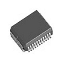
IDT728980J IDT, Integrated Device Technology Inc, IDT728980J Datasheet - Page 2

IDT728980J
Manufacturer Part Number
IDT728980J
Description
IC DGTL SW 256X256 44-PLCC
Manufacturer
IDT, Integrated Device Technology Inc
Series
7200r
Type
Multiplexerr
Datasheet
1.IDT728980J8.pdf
(10 pages)
Specifications of IDT728980J
Circuit
1 x 8:8
Independent Circuits
1
Voltage Supply Source
Single Supply
Voltage - Supply
4.75 V ~ 5.25 V
Operating Temperature
-40°C ~ 85°C
Mounting Type
Surface Mount
Package / Case
44-PLCC
Lead Free Status / RoHS Status
Contains lead / RoHS non-compliant
Current - Output High, Low
-
Lead Free Status / RoHS Status
Not Compliant, Contains lead / RoHS non-compliant
Other names
728980J
Available stocks
Company
Part Number
Manufacturer
Quantity
Price
Company:
Part Number:
IDT728980J
Manufacturer:
IDT, Integrated Device Technology Inc
Quantity:
10 000
Company:
Part Number:
IDT728980J8
Manufacturer:
IDT, Integrated Device Technology Inc
Quantity:
10 000
Company:
Part Number:
IDT728980JG
Manufacturer:
IDT, Integrated Device Technology Inc
Quantity:
10 000
Company:
Part Number:
IDT728980JG8
Manufacturer:
IDT, Integrated Device Technology Inc
Quantity:
10 000
NOTE:
1. DNC - Do Not Connect.
IDT728980 Time Slot Interchange
Digital Switch 256 x 256
SYMBOL
GND
VCC
DTA
RX0-7
F0i
C4i
A0-A5
DS
R/W
CS
D0-D7
TX0-7
ODE
CCO
INDEX
RX7
RX3
RX4
RX5
RX6
V
C4i
F0i
CC
A
A
A
0
1
2
PLCC: 0.05in. pitch, 0.65in. x 0.65in.
Ground.
VCC
Data Acknowledgment
(Open Drain)
RX Input 0 to 7
Frame Pulse
Clock
Address 0 to 5
Data Strobe
Read/Write
Chip Select
Data Bus 0 to 7
TX Outputs 0 to 7
(Three-state Outputs)
Output Drive Enable
Control Channel Output
10
11
12
13
14
15
16
17
7
8
9
(J44-1, order code: J)
NAME
TOP VIEW
I/O
I/O These pins provide microprocessor access to data in the internal control register. Connection Memory HIGH,
O
O
O
39
38
37
36
35
34
33
32
30
29
I
I
I
I
I
I
I
I
31
5706 drw02
TX3
Ground Rail.
+5.0 Volt Power Supply.
This active LOW output indicates that a data bus transfer is complete. A pull-up resistor is required at this
output.
Serial data input streams. These streams have 32 channels at data rates of 2.048 Mb/s.
This input identifies frame synchronization signals formatted to ST-BUS
4.096 MHz serial clock for shifting data in and out of the data streams.
These lines provide the address to IDT728980 internal registers.
This is the input for the active HIGH data strobe on the microprocessor interface. This input operates with
CS to enable the internal read and write generation.
This input controls the direction of the data bus lines (D0-D7) during a microprocessor access.
Active LOW input enabling a microprocessor read or write of control register or internal memories.
Connection Memory LOW and data memory.
Serial data output streams. These streams are composed of 32, 64 Kbit/s channels at data rates of 2.048 Mb/s.
This is an output enable for the TX0-7 serial outputs. If this input is LOW, TX0-7 are high-impedance. If this is
HIGH, each channel may still be put into high-impedance by software control.
This output is a 2.048 Mb/s line which contains 256 bits per frame. The level of each bit is controlled by the
contents of the CCO bit in the Connection Memory HIGH locations.
TX4
TX5
TX6
TX7
GND
D
D
D
D
D
0
1
2
3
4
PLASTIC DIP: 0.10in. pitch, 2.05in. x 0.60in.
DTA
RX0
RX1
RX2
RX3
RX4
RX5
RX6
RX7
V
R/W
C4i
DS
CC
F0i
A
A
A
A
A
A
0
1
2
3
4
5
1
2
3
4
5
6
7
8
9
10
11
12
13
14
15
16
17
18
19
20
(P40-1, order code: P)
TOP VIEW
2
5706 drw04
40
39
38
37
36
35
34
33
32
31
30
29
28
27
26
25
24
23
22
21
DESCRIPTION
CCO
ODE
TX0
TX1
TX2
TX3
TX4
TX5
TX6
TX7
GND
D
D
D
D
D
D
D
D
CS
0
1
2
3
4
5
6
7
INDEX
RX3
RX4
RX5
RX6
RX7
V
C4i
F0i
CC
A
A
A
0
1
2
PQFP: 0.80mm pitch, 10mm x 10mm
1
2
3
4
5
6
7
8
9
10
11
Commercial Temperature Range
(DB44-1, order code: DB)
®
specifications.
TOP VIEW
33
32
31
30
29
28
27
26
25
24
23
5706 drw03
TX3
TX4
TX5
TX6
TX7
GND
D
D
D
D
D
0
1
2
3
4


