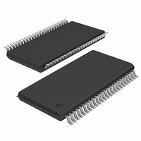
IDT74SSTV16857PAG8 IDT, Integrated Device Technology Inc, IDT74SSTV16857PAG8 Datasheet - Page 6

IDT74SSTV16857PAG8
Manufacturer Part Number
IDT74SSTV16857PAG8
Description
IC BUFFER 14BIT SSTL I/O 48TSSOP
Manufacturer
IDT, Integrated Device Technology Inc
Series
74SSTVr
Datasheet
1.IDT74SSTV16857PAG.pdf
(7 pages)
Specifications of IDT74SSTV16857PAG8
Logic Type
Registered Buffer with SSTL_2 Inputs and Outputs
Supply Voltage
2.3 V ~ 2.7 V
Number Of Bits
14
Operating Temperature
0°C ~ 70°C
Mounting Type
Surface Mount
Package / Case
48-TSSOP
Logic Family
SSTV
Logical Function
Registered Buffer
Number Of Elements
1
Number Of Inputs
14
Number Of Outputs
14
High Level Output Current
-20mA
Low Level Output Current
20mA
Propagation Delay Time
2.8ns
Operating Supply Voltage (typ)
2.5V
Operating Supply Voltage (max)
2.7V
Operating Supply Voltage (min)
2.3V
Clock-edge Trigger Type
Posit/Negat-Edge
Polarity
Non-Inverting
Technology
CMOS
Frequency (max)
220(Min)MHz
Mounting
Surface Mount
Pin Count
48
Operating Temp Range
-40C to 85C
Operating Temperature Classification
Industrial
Lead Free Status / RoHS Status
Lead free / RoHS Compliant
Other names
74SSTV16857PAG8
NOTES:
1. C
2. I
3. All input pulses are supplied by generators having the following characteristics: PRR ≤10MHz, Z
4. The outputs are measured one at a time with one transition per measurement.
5. V
6. V
7. V
8. t
TEST CIRCUITS AND WAVEFORMS
FOR PC1600-PC2700, V
FOR PC3200, V
LVCMOS
IDT74SSTV16857
14-BIT REGISTERED BUFFER WITH SSTL I/O
Input
Timing
RESET
(see note 2)
I
DD
Input
PLH
Input
DD
Input
TT
IH
IL
L
= V
= V
includes probe and jig capacitance.
tested with clock and data inputs held at V
= V
and t
REF
REF
REF
PHL
t
INACT
Voltage Waveforms - Setup and Hold Times
+ 310mV (AC voltage levels) for differential inputs. V
- 310mV (AC voltage levels) for differential inputs. V
= V
are the same as t
DDQ
Voltage Waveforms - Pulse Duration
Inputs Active and Inactive Times
Voltage and Current Waveforms
/2
V
DD
V
/2
REF
V
10%
REF
t
SU
DD
PD
.
t
W
= 2.6V ± 0.1V
V
ICR
t
N
DD
or GND, and I
DD
From Output
Under Test
V
= 2.5V ± 0.2V
REF
V
V
DD
REF
/2
90%
O
t
ACT
IL
IH
= 0mA.
= GND for LVCMOS input.
= V
V
V
DD
V
IH
IL
V
V
V
0V
DD
I(PP)
IH
IL
for LVCMOS input.
Load Circuit
6
LVCMOS
RESET
Timing
Output
Output
Input
V
Input
O
TT
Voltage Waveforms - Propagation Delay Times
Voltage Waveforms - Propagation Delay Times
= 50Ω, input slew rate = 1 V/ns ±20% (unless otherwise specified).
R
Test Point
C
(see note 1)
L
L
= 50Ω
= 30 pF
t
PLH
V
ICR
V
TT
INDUSTRIAL TEMPERATURE RANGE
V
DD
/2
t
PHL
V
V
ICR
TT
V
t
PHL
TT
V
V
V
I(PP)
V
V
OH
OL
V
V
OH
OL
IH
IL


