SSTVA16857AGLFT IDT, Integrated Device Technology Inc, SSTVA16857AGLFT Datasheet - Page 2
SSTVA16857AGLFT
Manufacturer Part Number
SSTVA16857AGLFT
Description
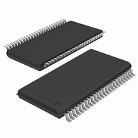
IC REGIST BUFF 14BIT DDR 48TSSOP
Manufacturer
IDT, Integrated Device Technology Inc
Specifications of SSTVA16857AGLFT
Logic Type
Registered Buffer for DDR
Number Of Bits
14
Mounting Type
Surface Mount
Package / Case
48-TSSOP
Lead Free Status / RoHS Status
Lead free / RoHS Compliant
Supply Voltage
-
Operating Temperature
-
Lead Free Status / Rohs Status
Supplier Unconfirmed


ICSSSTVA16857
General Description
Pin Configuration
0932A—05/12/04
The 14-bit ICSSSTVA16857 is a universal bus driver designed for 2.3V to 2.7V V
except for the LVCMOS RESET# input.
Data flow from D to Q is controlled by the differential clock (CLK/CLK#) and a control signal (RESET#). The positive edge
of CLK is used to trigger the data flow and CLK# is used to maintain sufficient noise margins where as RESET#, an
LVCMOS asynchronous signal, is intended for use at the time of power-up only. ICSSSTVA16857 supports low-power
standby operation. A logic level “Low” at RESET# assures that all internal registers and outputs (Q) are reset to the logic
“Low” state, and all input receivers, data (D) and clock (CLK/CLK#) are switched off. Please note that RESET# must always
be supported with LVCMOS levels at a valid logic state because VREF may not be stable during power-up.
To ensure that outputs are at a defined logic state before a stable clock has been supplied, RESET# must be held at a logic
“Low” level during power up.
In the DDR DIMM application, RESET# is specified to be completely asynchronous with respect to CLK and CLK#.
Therefore, no timing relationship can be guaranteed between the two signals. When entering a low-power standby state,
the register will be cleared and the outputs will be driven to a logic “Low” level quickly relative to the time to disable the
differential input receivers. This ensures there are no glitches on the output. However, when coming out of low-power
standby state, the register will become active quickly relative to the time to enable the differential input receivers. When
the data inputs are at a logic level “Low” and the clock is stable during the “Low”-to-”High” transition of RESET# until the
input receivers are fully enabled, the design ensures that the outputs will remain at a logic “Low” level.
2
2
3
1
, 4
, 5
, 2
, 4
, 5
P
4
, 3
, 3
N I
2
2
3
2
2
, 9
1
, 6
, 3
, 6
, 3
, 7
, 8
, 8
, 4
4
N
1
, 4
, 5
2
2
4
3
3
3
3
3
3
U
, 2
1
1
, 0
, 9
, 0
, 6
8
9
, 7
4
5
, 3
, 1
M
4
, 2
1
, 7
1
3
4
B
4
4
, 6
2
1
1
, 9
, 0
, 1
6
5
E
, 0
, 2
4
2
R
8
1
3
4
1
, 7
, 8
, 1
, 2
P
R
Q
N I
D
V
V
C
E
G
V
C
1 (
D
1 (
R
L
S
N
D
N
L
D
K
E
: 4
: 4
E
A
K
D
D
Q
#
F
T
) 1
M
) 1
#
E
O
N I
N I
N I
N I
N I
T
U
P
P
P
Y
T
W
W
P
P
P
W
P
P
P
P
U
U
U
U
U
R
R
R
E
U
T
T
T
T
T
T
D
D
P
N
R
n I
G
O
C
2
o
a
a
e
e
o
o r
u
p
s
a t
a t
g
e r
s
p t
t u
i t i
u
t e
a
n
t u
o
n i
e v
i t
s
e r
d
e v
a (
u
u
p
s
e f
p t
p
c
t u
i t c
u
p
e r
o l
c
t u
p
y l
o l
e v
p
k c
n
k c
y l
c
v
o l
e
l o
n i
v
n i
w
a t
l o
v
p
l o
p
t u
)
a t
g
t u
a t
e
g
g
e
D
e
DD
E
S
operation and SSTL_2 I/O levels,
C
R
P I
I T
O
N
Related parts for SSTVA16857AGLFT
Image
Part Number
Description
Manufacturer
Datasheet
Request
R

Part Number:
Description:
TRANSLATION DEVICE DPI 80-PQFP
Manufacturer:
IDT, Integrated Device Technology Inc
Datasheet:
Part Number:
Description:
IDT PART
Manufacturer:
IDT, Integrated Device Technology Inc
Datasheet:
Part Number:
Description:
IC LIU T1/E1/J1 OCTAL 256PBGA
Manufacturer:
IDT, Integrated Device Technology Inc
Datasheet:

Part Number:
Description:
IC FREQ TIMING GENERATOR 28TSSOP
Manufacturer:
IDT, Integrated Device Technology Inc
Datasheet:
Part Number:
Description:
IC CLK DVR PLL 1:10 40VFQFPN
Manufacturer:
IDT, Integrated Device Technology Inc
Datasheet:
Part Number:
Description:
IC CLK FANOUT BUFFER 1:18 32LQFP
Manufacturer:
IDT, Integrated Device Technology Inc
Datasheet:
Part Number:
Description:
IC CLK FANOUT BUFFER 1:18 32LQFP
Manufacturer:
IDT, Integrated Device Technology Inc
Datasheet:
Part Number:
Description:
IC CK505 VREG/RES 56TSSOP
Manufacturer:
IDT, Integrated Device Technology Inc
Datasheet:

Part Number:
Description:
IC SDRAM CLK DVR 1:10 48-TSSOP
Manufacturer:
IDT, Integrated Device Technology Inc
Datasheet:

Part Number:
Description:
IC CLK DVR PLL 1:10 48TSSOP
Manufacturer:
IDT, Integrated Device Technology Inc
Datasheet:
Part Number:
Description:
IC FLEXPC CLK PROGR P4 56-TSSOP
Manufacturer:
IDT, Integrated Device Technology Inc
Datasheet:
Part Number:
Description:
IC FLEXPC CLK PROGR P4 56-TSSOP
Manufacturer:
IDT, Integrated Device Technology Inc
Datasheet:
Part Number:
Description:
IC FLEXPC CLK PROGR P4 56-SSOP
Manufacturer:
IDT, Integrated Device Technology Inc
Datasheet:

Part Number:
Description:
IC PLL CLK DRIVER 2.5V 28-TSSOP
Manufacturer:
IDT, Integrated Device Technology Inc
Datasheet:
Part Number:
Description:
IC CLOCK DRIVER 2.5V 24-TSSOP
Manufacturer:
IDT, Integrated Device Technology Inc
Datasheet: