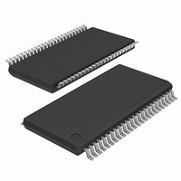
SSTVA16857AGLFT IDT, Integrated Device Technology Inc, SSTVA16857AGLFT Datasheet - Page 8

SSTVA16857AGLFT
Manufacturer Part Number
SSTVA16857AGLFT
Description
IC REGIST BUFF 14BIT DDR 48TSSOP
Manufacturer
IDT, Integrated Device Technology Inc
Specifications of SSTVA16857AGLFT
Logic Type
Registered Buffer for DDR
Number Of Bits
14
Mounting Type
Surface Mount
Package / Case
48-TSSOP
Lead Free Status / RoHS Status
Lead free / RoHS Compliant
Supply Voltage
-
Operating Temperature
-
Lead Free Status / Rohs Status
Supplier Unconfirmed
ICSSSTVA16857
0932A—05/12/04
Notes:
LVCMOS
RESET#
(see note 2)
Input
Timing
Input
Input
1. CL incluces probe and jig capacitance.
2. I
3. All input pulses are supplied by generators having the following characteristics: PRR @10 MHz,
Zo=50 , input slew rate = 1 V/ns ±20% (unless otherwise specified).
4. The outputs are measured one at a time with one transition per measurement.
5. V
6. V
7. V
8. t
Input
I
DD
t
DD
inact
PLH
TT
IH
IL
= V
tested with clock and data inputs held at V
= V
Voltage Waveforms - Setup and Hold Times
= V
and t
Voltage Waveforms - Pulse Duration
REF
REF
V
REF
Voltage and Current Waveforms
Inputs Active and Inactive Times
REF
10%
PHL
V
- 310mV (AC voltage levels) for differential inputs. V
+ 310mV (AC voltage levels) for differential inputs. V
Figure 1 - Parameter Measurement Information (V
DDQ
= V
are the same as t
/2
V
DDQ
REF
t
S
/2
t
w
V
ICR
t
h
pd
V
V
V
REF
REF
DDQ
From Output
/2
Under Test
90%
t
act
V
V
0 V
I
I
V
V
V
V
DDH
DDL
I(pp)
DDQ
IH
IL
IH
IL
Load Circuit
DDQ
8
LVCMOS
RESET#
or GND, and I
Timing
Output
Input
Output
Input
V
t
PHL
TT
Test Point
R =
Voltage Waveforms - Propagation Delay Times
(see Note 1)
L
C = 30 pF
Voltage Waveforms - Propagation Delay Times
L
50
IL
IH
DDQ
O
= GND for LVCMOS input.
V
= V
= 0 mA.
ICR
V
DD
= 2.5V ±0.2V)
DDQ
V
/2
TT
for LVCMOS input.
V
V
ICR
TT
t
PHL
V
TT
t
PHL
V
V
V
V
V
V
V
I(pp)
IH
OH
OL
OH
OL
IL


