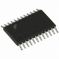
74LVXC3245MTC Fairchild Semiconductor, 74LVXC3245MTC Datasheet - Page 6

74LVXC3245MTC
Manufacturer Part Number
74LVXC3245MTC
Description
IC TRANSCVR TRI-ST 8BIT 24TSSOP
Manufacturer
Fairchild Semiconductor
Series
74LVXCr
Datasheet
1.74LVXC4245WMX.pdf
(9 pages)
Specifications of 74LVXC3245MTC
Logic Function
Translator, 3-State
Number Of Bits
8
Input Type
TTL
Output Type
Logic
Number Of Channels
8
Number Of Outputs/channel
1
Differential - Input:output
No/No
Propagation Delay (max)
4.8ns
Voltage - Supply
2.7 V ~ 3.6 V, 3 V ~ 5.5 V
Operating Temperature
-40°C ~ 85°C
Package / Case
24-TSSOP
Supply Voltage
*
Logic Type
CMOS
Logic Family
74LVX
Number Of Channels Per Chip
8
Input Level
CMOS
Output Level
CMOS
High Level Output Current
- 24 mA
Low Level Output Current
24 mA
Propagation Delay Time
8.5 ns
Supply Voltage (max)
3.6 V, 5.5 V
Supply Voltage (min)
2.7 V, 3 V
Maximum Operating Temperature
+ 85 C
Function
Transceiver
Input Bias Current (max)
8 uA
Minimum Operating Temperature
- 40 C
Mounting Style
SMD/SMT
Number Of Circuits
2
Polarity
Non-Inverting
Dc
PAEAB
Lead Free Status / RoHS Status
Lead free / RoHS Compliant
Data Rate
-
Lead Free Status / Rohs Status
Lead free / RoHS Compliant
Available stocks
Company
Part Number
Manufacturer
Quantity
Price
Part Number:
74LVXC3245MTC
Manufacturer:
FAIRCHILD/仙童
Quantity:
20 000
Company:
Part Number:
74LVXC3245MTCX
Manufacturer:
DONGBAO
Quantity:
16 606
Part Number:
74LVXC3245MTCX
Manufacturer:
FAIRCHILD/仙童
Quantity:
20 000
www.fairchildsemi.com
74LVXC3245
Power Up Considerations
To insure the system does not experience unnecessary I
current draw, bus contention, or oscillations during power
up, the following guidelines should be adhered to (refer to
Table 1):
• Power up the control side of the device first. This is the
• OE should ramp with or ahead of V
• The Transmit/Receive control pin (T/R) should ramp with
Please reference Application Note AN-5001 for more detailed information on using Fairchild’s LVX Low Voltage Dual
Supply CMOS Translating Transceivers.
Configurable I/O Application for PCMCIA Cards
Block Diagram
The LVXC3245 is a 24-pin dual supply device well suited
for PCMCIA configurable I/O applications. Ideal for low
power notebook designs, the LVXC3245 consumes less
than 1 mW of quiescent power in all modes of operation.
The LVXC3245 meets all PCMCIA I/O voltage require-
ments at 5V and 3.3V operation. By tying V
LVXC3245 to the card voltage supply, the PCMCIA card
Device Type
V
guard against bus contention.
V
CCA
CCA
, this will ensure that the A Port data pins are con-
side.
(power up 1st)
V
3V
CCA
TABLE 1. Low Voltage Translator Power Up Sequencing Table
configurable
3V to 5.5V
V
CCB
CCA
. This will help
CCB
with V
ramp
T/R
of the
CCA
CC
6
• A side data inputs should be driven to a valid logic level.
The above steps will ensure that no bus contention or oscil-
lations, and therefore no excessive current draw occurs
during the power up cycling of these devices. These steps
will help prevent possible damage to the translator devices
and potential damage to other system components.
will always experience rail to rail output swings, maximizing
the reliability of the interface.
The V
3V power supply. This voltage connection provides internal
references needed to account for variations in V
connected as in the figure above, the LVXC3245 meets all
the voltage and current requirements of the ISA bus stan-
dard (IEEE P996).
with V
figured as inputs. With V
I/O Port should be configured as inputs to help guard
against bus contention and oscillations.
This will prevent excessive current draw.
ramp
OE
CCA
CCA
pin on the LVXC3245 must always be tied to a
0V or V
A Side I/O
logic
CCA
CCA
receiving power first, the A
B Side I/O
outputs
I/O’s w/ OE HIGH
yes, V
Floatable Pin
CCB
Allowed
. When
CCB
and B


