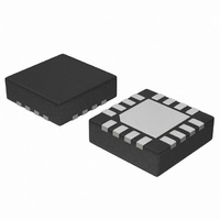
NCN4555MNG ON Semiconductor, NCN4555MNG Datasheet - Page 6

NCN4555MNG
Manufacturer Part Number
NCN4555MNG
Description
IC LEVEL SHIFTER SIM CARD 16-QFN
Manufacturer
ON Semiconductor
Datasheet
1.NCN4555MNR2G.pdf
(12 pages)
Specifications of NCN4555MNG
Logic Function
Level Shifter
Input Type
Logic
Output Type
Logic
Differential - Input:output
No/No
Voltage - Supply
1.8 V ~ 5.5 V
Operating Temperature
-25°C ~ 85°C
Package / Case
16-TFQFN Exposed Pad
Supply Voltage
1.8 V ~ 5.5 V
Mounting Style
SMD/SMT
Lead Free Status / RoHS Status
Lead free / RoHS Compliant
Number Of Channels
-
Data Rate
-
Lead Free Status / Rohs Status
Lead free / RoHS Compliant
Available stocks
Company
Part Number
Manufacturer
Quantity
Price
Company:
Part Number:
NCN4555MNG
Manufacturer:
ON Semiconductor
Quantity:
1
NOTE: Device will meet the specifications after thermal equilibrium has been established when mounted in a test socket or printed circuit
10. All the dynamic specifications (AC specifications) are guaranteed by design over the operating temperature range.
SIM INTERFACE SECTION
Pin
11
9
8
8
board with maintained transverse airflow greater than 500 lfpm. Electrical parameters are guaranteed only over the declared
operating temperature range. Functional operation of the device exceeding these conditions is not implied. Device specification limit
values are applied individually under normal operating conditions and not valid simultaneously.
R
SIM_RST
SIM_CLK
Symbol
SIM_I/O
pu_SIM_I/O
SIM_V
SIM_V
SIM_V
SIM_V
SIM_V
Output V
Output V
SIM_I/O Rise Time @ C
SIM_I/O Fall Time @ C
SIM_V
Output V
Output V
SIM_I/O Rise Time @ C
SIM_I/O Fall Time @ C
Card I/O Pullup Resistor
CC
CC
CC
CC
CC
CC
OH
OL
OH
OL
= +3.0 V (MOD_V
= +1.8 V (MOD_V
= +3.0 V (MOD_V
= +1.8 V (MOD_V
= +3.0 V (MOD_V
= +1.8 V (MOD_V
Output RESET V
Output RESET V
Output RESET Rise Time @ Cout = 30 pF
Output RESET Fall Time @ Cout = 30 pF
Output RESET V
Output RESET V
Output RESET Rise Time @ Cout = 30 pF
Output RESET Fall Time @ Cout = 30 pF
Output Duty Cycle
Max Output Frequency
Output V
Output V
Output SIM_CLK Rise Time @ Cout = 30 pF
Output SIM_CLK Fall Time @ Cout = 30 pF
Output Duty Cycle
Max Output Frequency
Output V
Output V
Output SIM_CLK Rise Time @ Cout = 30 pF
Output SIM_CLK Fall Time @ Cout = 30 pF
(Note 10)
@ I
@ I
@ I
@ I
SIM_IO
SIM_IO
SIM_IO
SIM_IO
OH
OL
OH
OL
@ I
@ I
= +1 mA, V
= +1.0 mA, V
@ I
@ I
= −20 mA, V
= −20 mA, V
out
out
out
out
Rating
sim_clk
sim_clk
sim_clk
sim_clk
= 30 pF
= 30 pF
OH
OL
OH
OL
= 30 pF
= 30 pF
CC
CC
CC
CC
CC
CC
@ I
@ I
@ I
@ I
= High)
= Low)
= High)
= Low)
= High)
= High)
= +200 mA
= +200 mA
= −20 mA
= −20 mA
I/O
sim_rst
sim_rst
sim_rst
sim_rst
I/O
I/O
I/O
http://onsemi.com
= 0 V
= V
=V
= 0 V
DD
= +200 mA
= +200 mA
= −20 mA
= −20 mA
DD
6
0.9 * SIM_V
0.9 * SIM_V
0.9 * SIM_V
0.9 * SIM_V
0.8 * SIM_V
0.8 * SIM_V
Min
40
40
10
0
0
5
0
5
0
0
0
CC
CC
CC
CC
CC
CC
Typ
14
SIM_V
SIM_V
SIM_V
SIM_V
SIM_V
SIM_V
Max
0.4
0.4
0.4
0.4
0.4
0.3
60
18
18
60
18
18
18
1
1
1
1
1
1
1
1
CC
CC
CC
CC
CC
CC
Unit
MHz
MHz
kW
ns
ns
ns
ns
ms
ms
ms
ms
ms
ms
ms
ms
%
%
V
V
V
V
V
V
V
V
V
V
V
V


