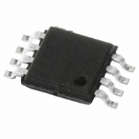
M95512-RDW6TP STMicroelectronics, M95512-RDW6TP Datasheet - Page 19

M95512-RDW6TP
Manufacturer Part Number
M95512-RDW6TP
Description
IC EEPROM 512KBIT 2MHZ 8TSSOP
Manufacturer
STMicroelectronics
Datasheet
1.M95512-RDW6TP.pdf
(48 pages)
Specifications of M95512-RDW6TP
Format - Memory
EEPROMs - Serial
Memory Type
EEPROM
Memory Size
512K (64K x 8)
Speed
2MHz
Interface
SPI, 3-Wire Serial
Voltage - Supply
1.8 V ~ 5.5 V
Operating Temperature
-40°C ~ 85°C
Package / Case
8-TSSOP
Organization
64 K x 8
Interface Type
SPI
Maximum Clock Frequency
2 MHz
Supply Voltage (max)
5.5 V
Supply Voltage (min)
1.8 V
Maximum Operating Current
3 mA
Maximum Operating Temperature
+ 85 C
Mounting Style
SMD/SMT
Minimum Operating Temperature
- 40 C
Operating Supply Voltage
2.5 V, 3.3 V, 5 V
Lead Free Status / RoHS Status
Lead free / RoHS Compliant
Other names
497-6358-2
M95512-RDW6TP
M95512-RDW6TP
Available stocks
Company
Part Number
Manufacturer
Quantity
Price
Company:
Part Number:
M95512-RDW6TP
Manufacturer:
STMicroelectronics
Quantity:
150 141
Company:
Part Number:
M95512-RDW6TP
Manufacturer:
ST
Quantity:
8 963
Part Number:
M95512-RDW6TP
Manufacturer:
ST
Quantity:
20 000
M95512-DR, M95512-W, M95512-R
6.3
6.3.1
6.3.2
6.3.3
6.3.4
Read Status Register (RDSR)
The Read Status Register (RDSR) instruction allows the Status Register to be read. The
Status Register may be read at any time, even while a Write or Write Status Register cycle
is in progress. When one of these cycles is in progress, it is recommended to check the
Write In Progress (WIP) bit before sending a new instruction to the device. It is also possible
to read the Status Register continuously, as shown in
The status and control bits of the Status Register are as follows:
WIP bit
The Write In Progress (WIP) bit indicates whether the memory is busy with a Write or Write
Status Register cycle. When set to 1, such a cycle is in progress, when reset to 0 no such
cycle is in progress.
WEL bit
The Write Enable Latch (WEL) bit indicates the status of the internal Write Enable Latch.
When set to 1 the internal Write Enable Latch is set, when set to 0 the internal Write Enable
Latch is reset and no Write or Write Status Register instruction is accepted.
BP1, BP0 bits
The Block Protect (BP1, BP0) bits are non-volatile. They define the size of the area to be
software protected against Write instructions. These bits are written with the Write Status
Register (WRSR) instruction. When one or both of the Block Protect (BP1, BP0) bits is set to
1, the relevant memory area (as defined in
(WRITE) instructions. The Block Protect (BP1, BP0) bits can be written provided that the
Hardware Protected mode has not been set.
SRWD bit
The Status Register Write Disable (SRWD) bit is operated in conjunction with the Write
Protect (W) signal. The Status Register Write Disable (SRWD) bit and Write Protect (W)
signal allow the device to be put in the Hardware Protected mode (when the Status Register
Write Disable (SRWD) bit is set to 1, and Write Protect (W) is driven low). In this mode, the
non-volatile bits of the Status Register (SRWD, BP1, BP0) become read-only bits and the
Write Status Register (WRSR) instruction is no longer accepted for execution.
Table 5.
Status Register Write Protect
SRWD
b7
Status register format
0
Doc ID 11124 Rev 14
0
0
Table
5) becomes protected against Write
BP1
Block Protect Bits
Figure
Write Enable Latch Bit
10.
BP0
WEL
Write In Progress Bit
Instructions
WIP
b0
19/48


