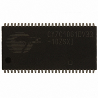
CY7C1061DV33-10ZSXI Cypress Semiconductor Corp, CY7C1061DV33-10ZSXI Datasheet - Page 10

CY7C1061DV33-10ZSXI
Manufacturer Part Number
CY7C1061DV33-10ZSXI
Description
IC SRAM 16MBIT 10NS 54TSOP
Manufacturer
Cypress Semiconductor Corp
Type
Asynchronousr
Datasheet
1.CY7C1061DV33-10ZSXI.pdf
(17 pages)
Specifications of CY7C1061DV33-10ZSXI
Memory Size
16M (1M x 16)
Package / Case
54-TSOP II
Format - Memory
RAM
Memory Type
SRAM - Asynchronous
Speed
10ns
Interface
Parallel
Voltage - Supply
3 V ~ 3.6 V
Operating Temperature
-40°C ~ 85°C
Access Time
10 ns
Supply Voltage (max)
4.6 V
Supply Voltage (min)
2 V
Maximum Operating Current
175 mA
Organization
1 M x 16
Maximum Operating Temperature
+ 85 C
Minimum Operating Temperature
- 40 C
Mounting Style
SMD/SMT
Number Of Ports
1
Operating Supply Voltage
3.3 V
Density
16Mb
Access Time (max)
10ns
Sync/async
Asynchronous
Architecture
Not Required
Clock Freq (max)
Not RequiredMHz
Operating Supply Voltage (typ)
3.3V
Address Bus
20b
Package Type
TSOP-II
Operating Temp Range
-40C to 85C
Supply Current
175mA
Operating Supply Voltage (min)
3V
Operating Supply Voltage (max)
3.6V
Operating Temperature Classification
Industrial
Mounting
Surface Mount
Pin Count
54
Word Size
16b
Number Of Words
1M
Rohs Compliant
YES
Lead Free Status / RoHS Status
Lead free / RoHS Compliant
Lead Free Status / RoHS Status
Lead free / RoHS Compliant, Lead free / RoHS Compliant
Other names
428-2960-5
CY7C1061DV33-10ZSXI
CY7C1061DV33-10ZSXI
Available stocks
Company
Part Number
Manufacturer
Quantity
Price
Company:
Part Number:
CY7C1061DV33-10ZSXI
Manufacturer:
CYPRES21
Quantity:
76
Part Number:
CY7C1061DV33-10ZSXI
Manufacturer:
CYPRESS/赛普拉斯
Quantity:
20 000
Switching Waveforms
Notes
Document Number: 38-05476 Rev. *G
19. For all packages except -BV1XI, CE is the logical combination of CE
20. WE is HIGH for read cycle.
21. Address valid before or similar to CE transition LOW.
22. Data I/O is high impedance if OE, BHE, and/or BLE = V
23. If CE goes HIGH simultaneously with WE going HIGH, the output remains in a high-impedance state.
CE is HIGH. For -BV1XI package, CE refers to CE.
BHE, BLE
Address
Data I/O
Data Out
Current
Address
BHE, BLE
Supply
V
WE
CE
CC
OE
CE
High Impedance
(continued)
t
t
LZCE
PU
t
SA
Figure 8. Read Cycle No. 2 (OE Controlled)
Figure 9. Write Cycle No. 1 (CE Controlled)
t
ACE
t
t
LZBE
t
DBE
LZOE
t
IH
DOE
.
50%
t
AW
1
and CE
t
RC
t
WC
2
. When CE
t
SCE
t
PWE
1
t
BW
is LOW and CE
Data Valid
t
SD
[19, 20, 21]
[19, 22, 23]
2
is HIGH, CE is LOW; when CE
t
HD
t
HZOE
t
HA
t
t
HZCE
HZBE
CY7C1061DV33
t
PD
1
50%
is HIGH or CE
Impedance
Page 10 of 17
High
2
is LOW,
I
I
ICC
ISB
CC
SB
[+] Feedback


