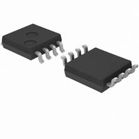
BR93L46RFVM-WTR Rohm Semiconductor, BR93L46RFVM-WTR Datasheet - Page 33

BR93L46RFVM-WTR
Manufacturer Part Number
BR93L46RFVM-WTR
Description
IC EEPROM 1KBIT 2MHZ 8MSOP
Manufacturer
Rohm Semiconductor
Datasheet
1.BR93L56RFVM-WTR.pdf
(41 pages)
Specifications of BR93L46RFVM-WTR
Format - Memory
EEPROMs - Serial
Memory Type
EEPROM
Memory Size
1K (64 x 16)
Speed
2MHz
Interface
Microwire, 3-Wire Serial
Voltage - Supply
1.8 V ~ 5.5 V
Operating Temperature
-40°C ~ 85°C
Package / Case
8-MSOP, Micro8™, 8-uMAX, 8-uSOP,
Lead Free Status / RoHS Status
Lead free / RoHS Compliant
Available stocks
Company
Part Number
Manufacturer
Quantity
Price
Company:
Part Number:
BR93L46RFVM-WTR
Manufacturer:
Rohm Semiconductor
Quantity:
24 984
Company:
Part Number:
BR93L46RFVM-WTR
Manufacturer:
MX
Quantity:
79
Part Number:
BR93L46RFVM-WTR
Manufacturer:
ROHM/罗姆
Quantity:
20 000
© 2011 ROHM Co., Ltd. All rights reserved.
BR93L□□-W Series, 93A□□-WM Series, BR93H□□-WC Series
www.rohm.com
4) When to directly connect DI and DO
(DO status)
○READY / BUSY status display (DO terminal)
(DO status)
This IC has independent input terminal DI and output terminal DO, and separate signals are handled on timing chart,
meanwhile, by inserting a resistance R between these DI and DO terminals, it is possible to carry out control by 1 control line.
○Data collision of microcontroller DI/O output and DO output and feedback of DO output to DI input.
(common to BR93H56-WC, BR93H66-WC, BR93H76-WC, BR93H86-WC)
This display outputs the internal status signal. When CS is started after tCS (Min.200ns)
from CS fall after write command input, “H” or “L” output.
R/B display=“L” (BUSY) = write under execution
accepted.
R/B display = “H” (READY) = command wait status
DI=“L” in the area
*Do not input any command while status signal is output. Command input in BUSY area is cancelled, but command input in READY area is accepted.
Therefore, status READY output is cancelled, and malfunction and mistake write may be made.
Drive from the microcontroller DI/O output to DI input on I/O timing, and signal output from DO output occur at the
same time in the following points.
4-1) 1 clock cycle to take in A0 address data at read command
Dummy bit “0” is output to DO terminal.
→When address data A0 = “1” input, through current route occurs.
After the timer circuit in the IC works and creates the period of tE/W, this time circuit completes automatically.
And write to the memory cell is made in the period of tE/W, and during this period, other command is not
Even after tE/W (max.10ms) from write of the memory cell, the following command is accepted.
Therefore, CS=“H” in the period of tE/W, and when input is in SK, DI, malfunction may occur, therefore,
CS=“H”. (Especially, in the case of shared input port, attention is required.)
CS
SK
DI
DO
High-Z
Fig.47 Collision timing at read data output at DI, DO direct connection
EEPROM CS input
EEPROM SK input
EEPROM DI input
EEPROM DO output
Microcontroller DI/O port
WRITE
INSTRUCTION
CLOCK
Fig.45 R/B status output timing chart
Fig.46 DI, DO control line common connection
Microcontroller
Microcontroller output
“H”
DI/O PORT
High-Z
A1
A1
R
t
SV
BUSY
A0
A0
STATUS
0
Microcontroller input
33/40
D15 D14 D13
DI
DO
EEPROM
Collision of DI input and DO output
READY
High-Z
Technical Note
2011.02 - Rev.F


