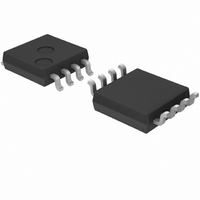
BR93L46RFVM-WTR Rohm Semiconductor, BR93L46RFVM-WTR Datasheet - Page 5

BR93L46RFVM-WTR
Manufacturer Part Number
BR93L46RFVM-WTR
Description
IC EEPROM 1KBIT 2MHZ 8MSOP
Manufacturer
Rohm Semiconductor
Datasheet
1.BR93L56RFVM-WTR.pdf
(41 pages)
Specifications of BR93L46RFVM-WTR
Format - Memory
EEPROMs - Serial
Memory Type
EEPROM
Memory Size
1K (64 x 16)
Speed
2MHz
Interface
Microwire, 3-Wire Serial
Voltage - Supply
1.8 V ~ 5.5 V
Operating Temperature
-40°C ~ 85°C
Package / Case
8-MSOP, Micro8™, 8-uMAX, 8-uSOP,
Lead Free Status / RoHS Status
Lead free / RoHS Compliant
Available stocks
Company
Part Number
Manufacturer
Quantity
Price
Company:
Part Number:
BR93L46RFVM-WTR
Manufacturer:
Rohm Semiconductor
Quantity:
24 984
Company:
Part Number:
BR93L46RFVM-WTR
Manufacturer:
MX
Quantity:
79
Part Number:
BR93L46RFVM-WTR
Manufacturer:
ROHM/罗姆
Quantity:
20 000
●Action timing characteristics
●Sync data input / output timing
© 2011 ROHM Co., Ltd. All rights reserved.
BR93L□□-W Series, 93A□□-WM Series, BR93H□□-WC Series
www.rohm.com
(BR93L□□-W, Ta=-40~+85℃, VCC=1.8~2.5V)
(BR93L□□-W, Ta=-40~+85℃, VCC=2.5~5.5V, BR93A□□-WM, Ta=-40~+105℃, VCC=2.5~5.5V)
○Data is taken by DI sync with the rise of SK.
○At read action, data is output from DO in sync with the rise of SK.
○The status signal at write (READY / BUSY) is output after tCS from the fall of CS after write command input, at the area
○After completion of each mode execution, set CS “L” once for internal circuit reset, and execute the following action mode.
SK frequency
SK “H” time
SK “L” time
CS “L” time
CS setup time
DI setup time
CS hold time
DI hold time
Data “1” output delay time
Data “0” output delay time
Time from CS to output establishment
Time from CS to High-Z
Write cycle time
SK frequency
SK “H” time
SK “L” time
CS “L” time
CS setup time
DI setup time
CS hold time
DI hold time
Data “1” output delay time
Data “0” output delay time
Time from CS to output establishment
Time from CS to High-Z
Write cycle time
DO where CS is “H”, and valid until the next command start bit is input. And, while CS is “L”, DO becomes High-Z.
DO(WRITE)
DO(READ)
Parameter
Parameter
CS
DI
SK
tDIS
tCSS
Fig.1 Sync data input / output timing
t PD0
tSKH
tDI H
Symbol
Symbol
STATUS VALID
t
t
t
t
t
t
t
t
t
t
t
t
t
t
t
t
t
t
f
t
CSH
t
t
f
t
CSH
t
t
SKH
SKL
CSS
PD1
PD0
E/W
SKH
SKL
CSS
PD1
PD0
E/W
DIH
DIH
DIS
DIS
SK
CS
SV
DF
SK
CS
SV
DF
tSKL
5/40
tPD1
Min.
Min.
230
230
200
100
100
200
100
100
0.8
0.8
50
0
1
0
-
-
-
-
-
-
-
-
-
-
-
-
2.5V≦VCC≦5.5V
1.8V≦VCC≦2.5V
Typ.
Typ.
tCSH
tDF
-
-
-
-
-
-
-
-
-
-
-
-
-
-
-
-
-
-
-
-
-
-
-
-
-
-
Max.
Max.
200
200
150
150
500
200
0.7
0.7
0.7
2
5
5
-
-
-
-
-
-
-
-
-
-
-
-
-
-
MHz
Unit
Unit
Technical Note
kHz
ms
ms
2011.02 - Rev.F
ns
ns
ns
ns
ns
ns
ns
ns
ns
ns
ns
us
us
us
ns
ns
ns
ns
us
us
us
ns


