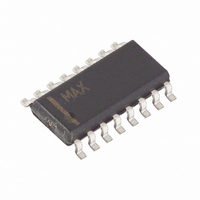
DS28E04S-100+ Maxim Integrated Products, DS28E04S-100+ Datasheet - Page 21

DS28E04S-100+
Manufacturer Part Number
DS28E04S-100+
Description
IC EEPROM 4KBIT 16SOIC
Manufacturer
Maxim Integrated Products
Datasheet
1.DS28E04S-100.pdf
(36 pages)
Specifications of DS28E04S-100+
Format - Memory
EEPROMs - Serial
Memory Type
EEPROM
Memory Size
4K (256 x 16)
Interface
1-Wire Serial
Operating Temperature
-40°C ~ 85°C
Package / Case
16-SOIC (3.9mm Width)
Organization
4 K x 1
Interface Type
1-Wire
Supply Voltage (max)
5.25 V
Supply Voltage (min)
2.8 V
Maximum Operating Current
1 mA
Maximum Operating Temperature
+ 85 C
Mounting Style
SMD/SMT
Minimum Operating Temperature
- 40 C
Lead Free Status / RoHS Status
Lead free / RoHS Compliant
Voltage - Supply
-
Speed
-
Lead Free Status / Rohs Status
Lead free / RoHS Compliant
PIO ACCESS WRITE [5Ah]
The PIO Access Write command is the only way to write to the PIO output-latch state register (address 0221h),
which controls the open-drain output transistors of the PIO channels. In an endless loop, this command first writes
new data to the PIO and then reads back the PIO status. The implicit read-after-write can be used by the master for
status verification. A PIO Access Write can be terminated at any time with a 1-Wire Reset. The state of the POL pin
does not affect this command.
After the command code, the master transmits a byte that determines the new state of the PIO output transistors.
The first (least significant) bit is associated to P0; the next bit affects P1. The other 6 bits of the new state byte do
not have corresponding PIO pins. These bits should always be transmitted as "1"s. To switch the output transistor
off (nonconducting) the corresponding bit value is 1. To switch the transistor on, that bit needs to be 0. This way the
data byte transmitted as the new PIO output state arrives in its true form at the PIO pins. To protect the
transmission against data errors, the master must repeat the new PIO byte in its inverted form. Only if the
transmission was error-free does the PIO status change. The actual PIO transition to the new state occurs with a
delay of t
is approximately 0.2µs. To inform the master about the successful change of the PIO status, the DS28E04-100
transmits a confirmation byte with the data pattern AAh. After the MS bit of the confirmation byte is transmitted, the
DS28E04-100 samples the status of the PIO pins, as shown in Figure 10, and sends it to the master. Depending on
the data the master can either continue writing more data to the PIO or issue a 1-Wire reset to end the command.
Figure 11. PIO Access Write Timing Diagram
PIO ACCESS PULSE [A5h]
As a convenient alternative to using PIO Access Write, the PIO Access Pulse command generates a self-timed
pulse on the selected PIO outputs. The polarity of the pulse is determined by the state of the POL pin. If POL = 1,
the pulse is negative (active low) and vice versa. The PIO Access Pulse command is accepted only if the device is
V
After the command code the master transmits a selection mask that specifies the PIO at which the pulse is to be
generated. A PIO is selected if the corresponding bit in the selection mask is a "1". The first (least significant) bit is
associated to P0; the next bit affects P1. The other 6 bits of the selection mask do not have corresponding PIO
pins. These bits should always be transmitted as "1"s. To protect the transmission against data errors, the master
must repeat the selection mask in its inverted form. Only if the transmission was error-free does the pulse occur.
The pulse begins with a delay of t
shown in Figure 12. The value of "x" is approximately 0.2µs. To inform the master about the successful pulse
generation, the DS28E04-100 transmits a confirmation byte with the data pattern AAh. While the last bit of the
confirmation byte is transmitted, the DS28E04-100 samples the status of the PIO pins, as shown in Figure 10, and
sends it to the master. Now the master can issue a 1-Wire reset to exit the command flow. This does not terminate
the pulse on a PIO pin.
CC
powered.
REH
+ x from the rising edge of the MS bit of the inverted PIO byte, as shown in Figure 11. The value of "x"
PIO
IO
Example - Old State = FEh, New state = FDh
REH
MS 2 bits of inverted
new-state byte
+ x from the rising edge of the MS bit of the inverted selection mask, as
FEh
t
REH
V
+x
21 of 36
TH
LS 2 bits of confir-
mation byte (AAh)
FDh


