DS1225Y-150+ Maxim Integrated Products, DS1225Y-150+ Datasheet - Page 2
DS1225Y-150+
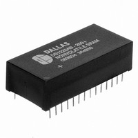
Manufacturer Part Number
DS1225Y-150+
Description
IC NVSRAM 64KBIT 150NS 28DIP
Manufacturer
Maxim Integrated Products
Datasheet
1.DS1225Y-200.pdf
(8 pages)
Specifications of DS1225Y-150+
Format - Memory
RAM
Memory Type
NVSRAM (Non-Volatile SRAM)
Memory Size
64K (8K x 8)
Speed
150ns
Interface
Parallel
Voltage - Supply
4.5 V ~ 5.5 V
Operating Temperature
0°C ~ 70°C
Package / Case
28-DIP Module (600 mil), 28-EDIP
Data Bus Width
8 bit
Organization
8 K x 8
Interface Type
Parallel
Access Time
150 ns
Supply Voltage (max)
5.5 V
Supply Voltage (min)
4.5 V
Maximum Operating Temperature
+ 70 C
Minimum Operating Temperature
0 C
Mounting Style
Through Hole
Lead Free Status / RoHS Status
Lead free / RoHS Compliant


READ MODE
The DS1225Y executes a read cycle whenever WE (Write Enable) is inactive (high) and CE (Chip
Enable) and OE (Output Enable) are active (low). The unique address specified by the 13 address inputs
(A
eight data output drivers within t
that CE and OE access times are also satisfied. If CE and OE access times are not satisfied, then data
access must be measured from the later-occurring signal and the limiting parameter is either t
or t
WRITE MODE
The DS1225Y executes a write cycle whenever the WE and CE signals are active (low) after address
inputs are stable. The later-occurring falling edge of CE or WE will determine the start of the write
cycle. The write cycle is terminated by the earlier rising edge of CE or WE . All address inputs must be
kept valid throughout the write cycle. WE must return to the high state for a minimum recovery time
(t
write cycles to avoid bus contention. However, if the output drivers are enabled ( CE and OE active) then
DATA RETENTION MODE
The DS1225Y provides full functional capability for V
nominal. Data is maintained in the absence of V
DS1225Y constantly monitors V
protects itself, all inputs become “don’t care,” and all outputs become high impedance. As V
below approximately 3.0 volts, a power switching circuit connects the lithium energy source to RAM to
retain data. During power-up, when V
connects external V
resume after V
NOT RECOMMENDED FOR NEW DESIGNS
WE will disable the outputs in t
WR
0
-A
OE
) before another cycle can be initiated. The OE control signal should be kept inactive (high) during
12
for OE rather than address access.
) defines which of the 8192 bytes of data is to be accessed. Valid data will be available to the
CC
exceeds 4.5 volts.
CC
to RAM and disconnects the lithium energy source. Normal RAM operation can
ODW
CC
ACC
. Should the supply voltage decay, the NV SRAM automatically write
from its falling edge.
(Access Time) after the last address input signal is stable, providing
CC
rises above approximately 3.0 volts, the power switching circuit
2 of 8
CC
CC
without any additional support circuitry. The
greater than 4.5 volts and write protects at 4.25
CO
DS1225Y
for CE
CC
falls
Related parts for DS1225Y-150+
Image
Part Number
Description
Manufacturer
Datasheet
Request
R

Part Number:
Description:
Manufacturer:
Maxim Integrated Products
Datasheet:
Part Number:
Description:
64K Nonvolatile SRAM
Manufacturer:
Maxim Integrated Products

Part Number:
Description:
IC NVSRAM 64KBIT 200NS 28DIP
Manufacturer:
Maxim Integrated Products
Datasheet:
Part Number:
Description:
NVRAM
Manufacturer:
Maxim Integrated Products
Datasheet:
Part Number:
Description:
MAX7528KCWPMaxim Integrated Products [CMOS Dual 8-Bit Buffered Multiplying DACs]
Manufacturer:
Maxim Integrated Products
Datasheet:
Part Number:
Description:
Single +5V, fully integrated, 1.25Gbps laser diode driver.
Manufacturer:
Maxim Integrated Products
Datasheet:
Part Number:
Description:
Single +5V, fully integrated, 155Mbps laser diode driver.
Manufacturer:
Maxim Integrated Products
Datasheet:
Part Number:
Description:
VRD11/VRD10, K8 Rev F 2/3/4-Phase PWM Controllers with Integrated Dual MOSFET Drivers
Manufacturer:
Maxim Integrated Products
Datasheet:
Part Number:
Description:
Highly Integrated Level 2 SMBus Battery Chargers
Manufacturer:
Maxim Integrated Products
Datasheet:
Part Number:
Description:
Current Monitor and Accumulator with Integrated Sense Resistor; ; Temperature Range: -40°C to +85°C
Manufacturer:
Maxim Integrated Products
Part Number:
Description:
TSSOP 14/A�/RS-485 Transceivers with Integrated 100O/120O Termination Resis
Manufacturer:
Maxim Integrated Products
Part Number:
Description:
TSSOP 14/A�/RS-485 Transceivers with Integrated 100O/120O Termination Resis
Manufacturer:
Maxim Integrated Products
Part Number:
Description:
QFN 16/A�/AC-DC and DC-DC Peak-Current-Mode Converters with Integrated Step
Manufacturer:
Maxim Integrated Products
Part Number:
Description:
TDFN/A/65V, 1A, 600KHZ, SYNCHRONOUS STEP-DOWN REGULATOR WITH INTEGRATED SWI
Manufacturer:
Maxim Integrated Products
Part Number:
Description:
Integrated Temperature Controller f
Manufacturer:
Maxim Integrated Products