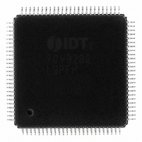
IDT70V9289L9PFI IDT, Integrated Device Technology Inc, IDT70V9289L9PFI Datasheet - Page 11

IDT70V9289L9PFI
Manufacturer Part Number
IDT70V9289L9PFI
Description
IC SRAM 1MBIT 9NS 100TQFP
Manufacturer
IDT, Integrated Device Technology Inc
Datasheet
1.IDT70V9289L9PFI.pdf
(19 pages)
Specifications of IDT70V9289L9PFI
Format - Memory
RAM
Memory Type
SRAM - Dual Port, Synchronous
Memory Size
1M (64K x 16)
Speed
9ns
Interface
Parallel
Voltage - Supply
3 V ~ 3.6 V
Operating Temperature
-40°C ~ 85°C
Package / Case
100-TQFP, 100-VQFP
Density
1Mb
Access Time (max)
20ns
Sync/async
Synchronous
Architecture
SDR
Clock Freq (max)
40MHz
Operating Supply Voltage (typ)
3.3V
Address Bus
32b
Package Type
TQFP
Operating Temp Range
-40C to 85C
Number Of Ports
2
Supply Current
240mA
Operating Supply Voltage (min)
3V
Operating Supply Voltage (max)
3.6V
Operating Temperature Classification
Industrial
Mounting
Surface Mount
Pin Count
100
Word Size
16b
Number Of Words
64K
Lead Free Status / RoHS Status
Contains lead / RoHS non-compliant
Other names
70V9289L9PFI
800-1401
800-1401
Available stocks
Company
Part Number
Manufacturer
Quantity
Price
Company:
Part Number:
IDT70V9289L9PFI
Manufacturer:
IDT, Integrated Device Technology Inc
Quantity:
10 000
Timing Waveform of Read Cycle for
Flow-Through Output (FT/PIPE
Timing Waveform of Read Cycle for Pipelined Operation
(FT/PIPE
NOTES:
1. Transition is measured 0mV from Low or High-impedance voltage with the Output Test Load (Figure 2).
2. OE is asynchronously controlled; all other inputs are synchronous to the rising clock edge.
3. ADS = V
4. The output is disabled (High-Impedance state) by CE
5. Addresses do not have to be accessed sequentially since ADS = V
6. If UB or LB was HIGH, then the Upper Byte and/or Lower Byte of DATA
7. "X' here denotes Left or Right port. The diagram is with respect to that port.
IDT70V9389/289L
High-Speed 3.3V 64K x18/x16 Dual-Port Synchronous Pipelined Static RAM
are for reference use only.
ADDRESS
DATA
IL
ADDRESS
, CNTEN and CNTRST = V
UB, LB
DATA
CLK
R/
CE
CE
OUT
UB, LB
OE
"X"
W
CLK
0
1
R/
CE
CE
OUT
(5)
(2)
OE
W
0
1
(5)
(2)
= V
t
t
t
t
SW
SB
SA
SC
IH
An
t
t
t
t
SC
SW
SB
SA
An
)
t
t
t
t
HC
HB
HW
HA
(3,7)
(1 Latency)
IH
t
t
t
t
HW
HC
HB
HA
t
CH2
.
t
t
CH1
CKLZ
t
(1)
CYC2
t
CD1
t
CYC1
t
CKLZ
0
t
CL2
= V
t
CL1
(1)
An + 1
IH
, CE
An + 1
1
"X"
= V
Qn
t
IL
CD2
t
DC
IL
constantly loads the address on the rising edge of the CLK; numbers
, UB = V
= V
OUT
6.42
for Qn + 2 would be disabled (High-Impedance state).
11
IL
IH
, or LB = V
)
(3,7)
An + 2
Qn
An + 2
IH
Qn + 1
t
following the next rising edge of the clock. Refer to Truth Table 1.
DC
t
OHZ
(1)
Industrial & Commercial Temperature Ranges
Qn + 1
t
t
OE
t
OLZ
OHZ
t
An + 3
t
(1)
SC
(4)
SB
(1)
(6)
t
t
An + 3
SC
SB
t
t
HC
Qn + 2
HB
t
t
HC
HB
t
DC
t
t
t
CKHZ
OE
OLZ
(1)
(1)
Qn + 2
4856 drw 06
4856 drw 07
(6)
..


