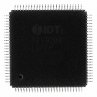
IDT70V9289L9PFI IDT, Integrated Device Technology Inc, IDT70V9289L9PFI Datasheet

IDT70V9289L9PFI
Specifications of IDT70V9289L9PFI
800-1401
Available stocks
Related parts for IDT70V9289L9PFI
IDT70V9289L9PFI Summary of contents
Page 1
... Features: True Dual-Ported memory cells which allow simultaneous access of the same memory location High-speed clock to data access – Commercial: 6/7.5/9/12ns (max.) – Industrial: 9ns (max.) Low-power operation – IDT70V9389/289L Active: 500mW (typ.) Standby: 1.5mW (typ.) Flow-Through or Pipelined output mode on either port via ...
Page 2
... The IDT70V9389/289 is a high-speed 64K x 18 (64K x 16) bit synchronous Dual-Port RAM. The memory array utilizes Dual-Port memory cells to allow simultaneous access of any address from both ports. Registers on control, data, and address inputs provide minimal setup and hold times. The timing latitude provided by this approach allows systems to be designed with very short cycle times ...
Page 3
IDT70V9389/289L High-Speed 3.3V 64K x18/x16 Dual-Port Synchronous Pipelined Static RAM Pin Configurations (1,2,3) 03/28/03 INDEX 100 ...
Page 4
IDT70V9389/289L High-Speed 3.3V 64K x18/x16 Dual-Port Synchronous Pipelined Static RAM Pin Configurations (1,2,3) 03/28/ ...
Page 5
IDT70V9389/289L High-Speed 3.3V 64K x18/x16 Dual-Port Synchronous Pipelined Static RAM Pin Configurations (1,2,3) 03/28/03 Index 100 ...
Page 6
IDT70V9389/289L High-Speed 3.3V 64K x18/x16 Dual-Port Synchronous Pipelined Static RAM Pin Names Left Port Right Port Chip Enables 0L, 1L 0R, 1R R/W R/W Read/Write Enable Output Enable ...
Page 7
IDT70V9389/289L High-Speed 3.3V 64K x18/x16 Dual-Port Synchronous Pipelined Static RAM Truth Table II—Address Counter Control Previous Internal External Internal Address Address Address Used CLK ↑ ↑ ↑ ↑ ...
Page 8
IDT70V9389/289L High-Speed 3.3V 64K x18/x16 Dual-Port Synchronous Pipelined Static RAM DC Electrical Characteristics Over the Operating Temperature and Supply Voltage Range Symbol Parameter ( Input Leakage Current Output Leakage Current LO V Output Low Voltage ...
Page 9
IDT70V9389/289L High-Speed 3.3V 64K x18/x16 Dual-Port Synchronous Pipelined Static RAM AC Test Conditions Input Pulse Levels Input Rise/Fall Times Input Timing Reference Levels Output Reference Levels Output Load DATA OUT 435Ω Figure 1. AC Output Test load. , tCD 1 ...
Page 10
IDT70V9389/289L High-Speed 3.3V 64K x18/x16 Dual-Port Synchronous Pipelined Static RAM AC Electrical Characteristics Over the Operating Temperature Range (Read and Write Cycle Timing) Symbol Parameter (2) t Clock Cycle Time (Flow-Through) CYC1 (2) t Clock Cycle Time (Pipelined) CYC2 (2) ...
Page 11
IDT70V9389/289L High-Speed 3.3V 64K x18/x16 Dual-Port Synchronous Pipelined Static RAM Timing Waveform of Read Cycle for Flow-Through Output (FT/PIPE t CH1 CLK UB ...
Page 12
IDT70V9389/289L High-Speed 3.3V 64K x18/x16 Dual-Port Synchronous Pipelined Static RAM Timing Waveform of a Bank Select Pipelined Read t CYC2 t CH2 CLK ADDRESS (B1 0(B1) DATA OUT(B1) t ...
Page 13
... Output state (High, Low, or High-impedance) is determined by the previous cycle control signals UB, LB, and ADS = V , CNTEN, and CNTRST = Addresses do not have to be accessed sequentially since ADS = V reference use only. 5. "NOP" is "No Operation." Data in memory at the selected address may be corrupted and should be re-written to guarantee data integrity. t CL2 ...
Page 14
... Output state (High, Low, or High-impedance) is determined by the previous cycle control signals UB, LB, and ADS = V , CNTEN, and CNTRST = Addresses do not have to be accessed sequentially since ADS = V reference use only. 5. "NOP" is "No Operation." Data in memory at the selected address may be corrupted and should be re-written to guarantee data integrity. t CL1 ...
Page 15
IDT70V9389/289L High-Speed 3.3V 64K x18/x16 Dual-Port Synchronous Pipelined Static RAM Timing Waveform of Pipelined Read with Address Counter Advance t CYC2 t t CH2 CL2 CLK ADDRESS SAD HAD ADS CNTEN (2) Qx ...
Page 16
IDT70V9389/289L High-Speed 3.3V 64K x18/x16 Dual-Port Synchronous Pipelined Static RAM Timing Waveform of Write with Address Counter Advance (Flow-Through or Pipelined Outputs) t CH2 CLK ADDRESS (3) INTERNAL ADDRESS t t SAD HAD ADS (7) ...
Page 17
... LOW to HIGH transition of the clock signal. An asynchronous output enable is provided to ease asynchronous bus interfacing. Counter enable inputs are also provided to staff the operation of the address counters for fast interleaved memory applications ...
Page 18
IDT70V9389/289L High-Speed 3.3V 64K x18/x16 Dual-Port Synchronous Pipelined Static RAM Ordering Information XXXXX Device Power Speed Package Type NOTES: 1. Industrial temperature range is available. For specific speeds, packages and powers contact your sales office. 2. Green ...
Page 19
IDT70V9389/289L High-Speed 3.3V 64K x18/x16 Dual-Port Synchronous Pipelined Static RAM Datasheet Document History 09/30/99: Initial Public Release 11/12/99: Replaced IDT logo 06/23/00: Page 3 Changed information in Truth Table II Page 4 Increased storage temperature parameters Clarified T Page 5 ...


