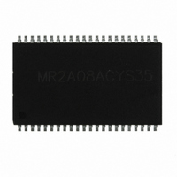
MR2A08ACYS35 EverSpin Technologies Inc, MR2A08ACYS35 Datasheet
MR2A08ACYS35
Specifications of MR2A08ACYS35
Available stocks


Related parts for MR2A08ACYS35


MR2A08ACYS35 Summary of contents
Page 1
... The MR2A08A provides highly reliable data storage over a wide range of temperatures. The product is offered with commercial temperature (0 to +70 °C), industrial temperature (-40 to +85 °C), and automotive temperature (-40 to +125 °C) range options. CONTENTS 1. DEVICE PIN ASSIGNMENT......................................................................... 2 2. ELECTRICAL SPECIFICATIONS................................................................. 4 3. TIMING SPECIFICATIONS.......................................................................... 7 4. ORDERING INFORMATION....................................................................... 11 5. MECHANICAL DRAWING.......................................................................... 12 6. REVISION HISTORY...................................................................................... 14 How to Reach Us.......................................................................................... 14 Everspin Technologies © 2009 512K x 8 MRAM Memory RoHS 1 Document Number: MR2A08A Rev. 4, 7/2009 MR2A08A ...
Page 2
... No Connection - Pin 2, 43 (TSOPII); Ball H6, G2 (BGA) Reserved For Future Expansion Everspin Technologies © 2009 Figure 1.1 Block Diagram OUTPUT ENABLE ROW COLUMN DECODER DECODER 8 SENSE AMPS 512k x 8 BIT MEMORY ARRAY FINAL 8 WRITE DRIVERS WRITE ENABLE Table 1.1 Pin Functions 2 Document Number: MR2A08A Rev. 4, 7/2009 MR2A08A 8 8 ...
Page 3
DEVICE PIN ASSIGNMENT Figure 1.2 Pin Diagrams for Available Packages (Top View ...
Page 4
ELECTRICAL SPECIFICATIONS Absolute Maximum Ratings This device contains circuitry to protect the inputs against damage caused by high static voltages or electric fields; however advised that normal precautions be taken to avoid application of any voltage greater than maximum rated voltages to these high-impedance (Hi-Z) circuits. The device also contains protection against external magnetic fields. Precautions should be taken to avoid application of any magnetic field more intense than the maximum field intensity specified in the maximum ratings. Parameter Supply voltage 2 Voltage on an pin 2 Output current per pin Package power dissipation Temperature under bias MR2A08A (Commercial) MR2A08AC (Industrial) MR2A08AM (Automotive) Storage Temperature Lead temperature during solder (3 minute max) Maximum magnetic field during write MR2A08A (All Temperatures) Maximum magnetic field during read or standby Permanent device damage may occur if absolute maximum ratings are exceeded. Functional opera- 1 tion should be restricted to recommended operating conditions. Exposure to excessive voltages or magnetic fields could affect device reliability. All voltages are referenced Power dissipation capability depends on package characteristics and use environment. 3 Everspin Technologies © 2009 Table 2.1 ...
Page 5
... Automotive temperature profile assumes 10% duty cycle at maximum temperature (2-years out of 20-year life) iv Power Up and Power Down Sequencing MRAM is protected from write operations whenever V there is a startup time before read or write operations can start. This time allows memory power supplies to stabilize. The E and W control signals should track V high for the startup time. In most systems, this means that these signals should be pulled up with a resis- tor so that signal remains high if the driving signal is Hi-Z during power up. Any logic that drives E and W should hold the signals high with a power-on reset signal for longer than the startup time. During power loss or brownout where V observed when power returns above V V ...
Page 6
Electrical Specifications Parameter Input leakage current Output leakage current Output low voltage ( mA +100 μA) OL Output high voltage ( mA -100 μA) OL Parameter AC active supply current - read modes ( mA max) OUT DD AC active supply current - write modes (V = max) DD MR2A08A (Commercial) MR2A08AC (Industrial) MR2A08AM (Automotive) AC standby current (V = max ...
Page 7
TIMING SPECIFICATIONS Parameter Address input capacitance Control input capacitance Input/Output capacitance f = 1.0 MHz 3 °C, periodically sampled rather than 100% tested Parameter Logic input timing measurement reference level Logic output timing measurement reference level Logic input pulse levels Input rise/fall time Output load for low and high impedance parameters Output load for all other timing parameters Output Everspin Technologies © 2009 Table 3.1 Capacitance Symbol Table 3.2 AC Measurement Conditions Figure 3.1 Output Load Test Low and ...
Page 8
Timing Specifications Read Mode Parameter Read cycle time Address access time Enable access time 2 Output enable access time Output hold from address change Enable low to output active 3 Output enable low to output active Enable high to output Hi-Z 3 Output enable high to output Hi high for read cycle. Power supplies must be properly grounded and decoupled, and bus contention conditions must be 1 minimized or eliminated during read or write cycles. Addresses valid before or at the same time E goes low. 2 This parameter is sampled and not 100% tested. Transition is measured ±200 mV from the steady-state voltage. 3 Everspin Technologies © 2009 Table 3.3 Read Cycle Timing Symbol t AVAV t AVQV t ELQV t GLQV ...
Page 9
Timing Specifications Parameter Write cycle time 2 Address set-up time Address valid to end of write (G high) Address valid to end of write (G low) Write pulse width (G high) Write pulse width (G low) Data valid to end of write Data hold time Write low to data Hi-Z 3 Write high to output active 3 Write recovery time All write occurs during the overlap of E low and W low. Power supplies must be properly grounded and decoupled and bus 1 contention conditions must be minimized or eliminated during read and write cycles goes low at the same time or after W goes low, the output will remain in a high impedance state. After has been brought high, the signal must remain in steady-state high for a minimum of 2 ns. The minimum time between E being asserted low in one cycle to E being asserted low in a subsequent cycle is the same as the minimum cycle time allowed for the device. All write cycle timings are referenced from the last valid address to the first transition address. 2 This parameter is sampled and not 100% tested. Transition is measured ±200 mV from the steady-state voltage. At any given 3 voltage or temperature, t (max) < t WLQZ Everspin Technologies © 2009 Table 3.4 Write Cycle Timing 1 (W Controlled) ...
Page 10
Timing Specifications Parameter Write cycle time 2 Address set-up time Address valid to end of write (G high) Address valid to end of write (G low) Enable to end of write (G high) Enable to end of write (G low) 3 Data valid to end of write Data hold time Write recovery time All write occurs during the overlap of E low and W low. Power supplies must be properly grounded and decoupled and bus 1 contention conditions must be minimized or eliminated during read and write cycles goes low at the same time or after W goes low, the output will remain in a high impedance state. After has been brought high, the signal must remain in steady-state high for a minimum of 2 ns. The minimum time between E being asserted low in one cycle to E being asserted low in a subsequent cycle is the same as the minimum cycle time allowed for the device. All write cycle timings are referenced from the last valid address to the first transition address goes low at the same time or after W goes low, the output will remain in a high-impedance state goes high at the 3 same time or before W goes high, the output will remain in a high-impedance state. Everspin Technologies © 2009 Table 3.5 Write Cycle Timing 2 (E Controlled) Symbol t AVAV t ...
Page 11
... ORDERING INFORMATION Part Number MR2A08AYS35 MR2A08ACYS35 MR2A08AMYS35 1 MR2A08AYS35R MR2A08ACYS35R MR2A08AMYS35R MR2A08AMA35 MR2A08ACMA35 MR2A08AMMA35 1 The automotive temperature grade parts are classified as Preliminary, a product in development 1 and/or qualification that has fixed target specifications that are subject to change pending charac- terization results. Everspin Technologies © 2009 Figure 4.1 Part Numbering System Table 4.1 Available Parts Description 3.3 V 512Kx8 MRAM 44-TSOP 3.3 V 512Kx8 MRAM 44-TSOP 3.3 V 512Kx8 MRAM 44-TSOP 3.3 V 512Kx8 MRAM 44-TSOP T&R 3.3 V 512Kx8 MRAM 44-TSOP T& ...
Page 12
MECHANICAL DRAWING 1. Dimensions and tolerances per ASME Y14.5M - 1994. 2. Dimensions in Millimeters. 3. Dimensions do not include mold protrusion. 4. Dimension does not include DAM bar protrusions. DAM Bar protrusion shall not cause the lead width to exceed 0.58. Everspin Technologies © 2009 Figure 5.1 TSOP-II Print Version Not To Scale 12 Document Number: MR2A08A Rev. 4, 7/2009 MR2A08A ...
Page 13
Mechanical Drawings BOTTOM VIEW 1. Dimensions in Millimeters. 2. Dimensions and tolerances per ASME Y14.5M - 1994. 3. Maximum solder ball diameter measured parallel to DATUM A 4. DATUM A, the seating plane is determined by the spherical crowns of the solder balls. 5. Parallelism measurement shall exclude any effect of mark on top surface of package. Everspin Technologies © 2009 Figure 5.2 FBGA TOP VIEW Print Version Not To Scale 13 MR2A08A SIDE VIEW Document Number: MR2A08A Rev. 4, 7/2009 ...
Page 14
REVISION HISTORY Revision Date 0 Oct 25, 2007 Initial Advance Information Release 1 Oct 29, 2007 2 Sep 12, 2008 3 Apr 10, 2009 4 July 6, 2009 Unless otherwise noted, this is a Production Product - This product conforms to specifications per the terms of the Everspin standard warranty. The product ...