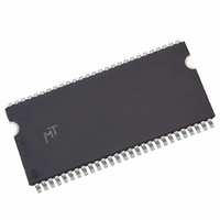
MT48LC16M8A2P-75 IT:G TR Micron Technology Inc, MT48LC16M8A2P-75 IT:G TR Datasheet - Page 30

MT48LC16M8A2P-75 IT:G TR
Manufacturer Part Number
MT48LC16M8A2P-75 IT:G TR
Description
IC SDRAM 128MBIT 133MHZ 54TSOP
Manufacturer
Micron Technology Inc
Datasheet
1.MT48LC8M16A2P-75G_TR.pdf
(74 pages)
Specifications of MT48LC16M8A2P-75 IT:G TR
Format - Memory
RAM
Memory Type
SDRAM
Memory Size
128M (16M x 8)
Speed
133MHz
Interface
Parallel
Voltage - Supply
3 V ~ 3.6 V
Operating Temperature
-40°C ~ 85°C
Package / Case
54-TSOP II
Lead Free Status / RoHS Status
Lead free / RoHS Compliant
Figure 17:
PDF: 09005aef8091e66d/Source: 09005aef8091e625
128MSDRAM_2.fm - Rev. N 1/09 EN
READ-to-PRECHARGE
Notes:
desired data element is valid, where x = CL - 1. This is shown in Figure 17 for each
possible CL; data element n + 3 is either the last of a burst of four or the last desired of a
longer burst. Following the PRECHARGE command, a subsequent command to the
same bank cannot be issued until
hidden during the access of the last data element(s).
In the case of a fixed-length burst being executed to completion, a PRECHARGE
command issued at the optimum time (as described above) provides the same operation
that would result from the same fixed-length burst with auto precharge. The disadvan-
tage of the PRECHARGE command is that it requires that the command and address
buses be available at the appropriate time to issue the command; the advantage of the
PRECHARGE command is that it can be used to truncate fixed-length or full-page bursts.
Full-page READ bursts can be truncated with the BURST TERMINATE command, and
fixed-length READ bursts may be truncated with a BURST TERMINATE command,
provided that auto precharge was not activated. The BURST TERMINATE command
should be issued x cycles before the clock edge at which the last desired data element is
valid, where x = CL - 1. This is shown in Figure 18 on page 31 for each possible CL; data
element n + 3 is the last desired data element of a longer burst.
COMMAND
COMMAND
1. DQM is LOW.
ADDRESS
ADDRESS
CLK
CLK
DQ
DQ
BANK a,
BANK a,
COL n
COL n
T0
T0
READ
READ
CL = 2
T1
T1
NOP
NOP
CL = 3
30
T2
T2
NOP
NOP
D
t
OUT
RP is met. Note that part of the row precharge time is
n
Micron Technology, Inc., reserves the right to change products or specifications without notice.
T3
T3
NOP
NOP
n + 1
D
D
OUT
OUT
n
TRANSITIONING DATA
PRECHARGE
PRECHARGE
(a or all)
(a or all)
T4
BANK
BANK
T4
X = 1 cycle
n + 2
D
n + 1
D
OUT
OUT
128Mb: x4, x8, x16 SDRAM
X = 2 cycles
T5
T5
NOP
NOP
n + 2
n + 3
D
D
OUT
OUT
t RP
t RP
©1999 Micron Technology, Inc. All rights reserved.
T6
T6
NOP
NOP
n + 3
D
OUT
DON’T CARE
Operations
BANK a,
BANK a,
ACTIVE
ACTIVE
T7
T7
ROW
ROW


