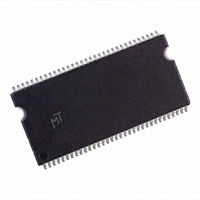
MT46V256M4P-6T:A TR Micron Technology Inc, MT46V256M4P-6T:A TR Datasheet - Page 28

MT46V256M4P-6T:A TR
Manufacturer Part Number
MT46V256M4P-6T:A TR
Description
IC DDR SDRAM 1GBIT 6NS 66TSOP
Manufacturer
Micron Technology Inc
Datasheet
1.MT46V256M4P-6TA_TR.pdf
(82 pages)
Specifications of MT46V256M4P-6T:A TR
Format - Memory
RAM
Memory Type
DDR SDRAM
Memory Size
1G (256M x 4)
Speed
6ns
Interface
Parallel
Voltage - Supply
2.3 V ~ 2.7 V
Operating Temperature
0°C ~ 70°C
Package / Case
66-TSOP
Lead Free Status / RoHS Status
Lead free / RoHS Compliant
Figure 10:
PDF: 09005aef80a2f898/Source: 09005aef82a95a3a
DDR_x4x8x16_Core2.fm - 1Gb DDR: Rev. I, Core DDR: Rev. B 12/07 EN
Derating Data Valid Window (
31. CK and CK# input slew rate must be ≥1 V/ns (≥2 V/ns if measured differentially).
32. DQ and DM input slew rates must not deviate from DQS by more than 10 percent. If
33. V
34. The clock is allowed up to ±150ps of jitter. Each timing parameter is allowed to vary by
35.
36. READs and WRITEs with auto precharge are not allowed to be issued until
37. Any positive glitch must be less than 1/3 of the clock cycle and not more than +400mV
38. Normal output drive curves:
38b. The driver pull-down current variation, within nominal voltage and temperature
38a. The full driver pull-down current variation from MIN to MAX process; tempera-
38c. The full driver pull-up current variation from MIN to MAX process; temperature
3.0ns
2.5ns
2.0ns
1.5ns
1.0ns
the DQ/DM/DQS slew rate is less than 0.5 V/ns, timing must be derated: 50ps must
be added to
-6T speed grades, the slew rate must be ≥0.5 V/ns. If the slew rate exceeds 4 V/ns,
functionality is uncertain.
the same amount.
t
and CK# inputs, collectively, during bank active.
can be satisfied prior to the internal PRECHARGE command being issued.
or 2.9V (+300mV or 2.9V maximum for -5B), whichever is less. Any negative glitch
must be less than 1/3 of the clock cycle and not exceed either
-5B), whichever is more positive. The average cannot be below the +2.5V (2.6V for -5B)
minimum.
HP (MIN) is the lesser of
DD
ture and voltage will lie within the outer bounding lines of the V-I curve of
Figure 11 on page 29.
limits, is expected, but not guaranteed, to lie within the inner bounding lines of
the V-I curve of Figure 11 on page 29.
and voltage will lie within the outer bounding lines of the V-I curve of Figure 12 on
page 29.
must not vary more than 4 percent if CKE is not active while any bank is active.
50/50
2.00
1.60
2.75
2.50
2.10
t
DS and
1.97
1.58
2.71
2.46
2.07
t
QH –
49/51
t
1.94
1.55
2.68
2.43
2.04
DH for each 100 mV/ns reduction in slew rate. For -5B and
t
t
CL (MIN) and
DQSQ)
28
1.91
1.53
2.64
2.39
2.01
Clock Duty Cycle
48/53
1.88
1.50
2.60
2.35
1.98
Micron Technology, Inc., reserves the right to change products or specifications without notice.
Electrical Specifications – DC and AC
1.85
1.48
2.56
2.31
1.95
t
CH (MIN) actually applied to the device CK
47/53
1.82
1.45
2.53
2.28
1.92
1Gb: x4, x8, x16 DDR SDRAM
1.79
1.43
2.49
2.24
1.89
46/54
1.76
1.40
©2003 Micron Technology, Inc. All rights reserved.
2.45
2.20
1.86
–
300mV or 2.2V (2.4V for
-6T @ t CK = 7.5ns
-75E / -75 @ t CK = 7.5ns
-6 @ t CK = 6ns
-6T @ t CK = 6ns
-5B @ t CK = 5ns
1.73
1.38
2.41
2.16
1.83
45/55
2.13
1.70
1.35
2.38
1.80
t
RAS (MIN)


