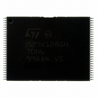
M29W128GH70N6E NUMONYX, M29W128GH70N6E Datasheet - Page 28

M29W128GH70N6E
Manufacturer Part Number
M29W128GH70N6E
Description
IC FLASH 128MBIT 70NS 56TSOP
Manufacturer
NUMONYX
Series
Axcell™r
Datasheet
1.M29W128GH70N6E.pdf
(94 pages)
Specifications of M29W128GH70N6E
Format - Memory
FLASH
Memory Type
FLASH
Memory Size
128M (16Mx8, 8Mx16)
Speed
70ns
Interface
Parallel
Voltage - Supply
2.7 V ~ 3.6 V
Operating Temperature
-40°C ~ 85°C
Package / Case
56-TSOP
Package
56TSOP
Cell Type
NOR
Density
128 Mb
Architecture
Sectored
Block Organization
Symmetrical
Typical Operating Supply Voltage
3|3.3 V
Sector Size
128KByte x 128
Timing Type
Asynchronous
Interface Type
Parallel
Lead Free Status / RoHS Status
Lead free / RoHS Compliant
Available stocks
Company
Part Number
Manufacturer
Quantity
Price
Company:
Part Number:
M29W128GH70N6E
Manufacturer:
Numonyx
Quantity:
17 280
Company:
Part Number:
M29W128GH70N6E
Manufacturer:
MICRON
Quantity:
595
Company:
Part Number:
M29W128GH70N6E
Manufacturer:
MICRON45
Quantity:
556
Part Number:
M29W128GH70N6E
Manufacturer:
ST
Quantity:
20 000
6.1.3
6.1.4
6.1.5
28/94
Read CFI Query command
The memory contains an information area, named CFI data structure, which contains a
description of various electrical and timing parameters, density information and functions
supported by the memory. See
Table 40
(CFI) memory area.
The Read CFI Query command is used to put the memory in read CFI query mode. Once in
read CFI query mode, bus read operations to the memory will output data from the common
flash interface (CFI) memory area. One bus write cycle is required to issue the Read CFI
Query command. This command is valid only when the device is in the read array or auto
select mode.
The Read/Reset command must be issued to return the device to the previous mode (the
read array mode or auto select mode). A second Read/Reset command is required to put
the device in read array mode from auto select mode.
Chip Erase command
The Chip Erase command can be used to erase the entire chip. Six bus write operations are
required to issue the Chip Erase command and start the program/erase controller.
If some block are protected, then these are ignored and all the other blocks are erased. If all
of the blocks are protected the Chip Erase operation appears to start but will terminate
within about 100 µs, leaving the data unchanged. No error condition is given when protected
blocks are ignored.
During the erase operation the memory will ignore all commands, including the Erase
Suspend command. It is not possible to issue any command to abort the operation. Typical
chip erase times are given in
operation will output the status register on the data inputs/outputs. See
register
After the chip erase operation has completed the memory will return to the read mode,
unless an error has occurred. When an error occurs the memory will continue to output the
status register. A Read/Reset command must be issued to reset the error condition and
return to read mode.
The Chip Erase command sets all of the bits in unprotected blocks of the memory to ’1’. All
previous data is lost.
The chip erase operation is aborted by performing a reset or powering down the device. In
this case, data integrity cannot be ensured, and it is recommended to erase again the entire
chip.
Block Erase command
The Block Erase command can be used to erase a list of one or more blocks. It sets all of
the bits in the unprotected selected blocks to ’1’. All previous data in the selected blocks is
lost.
Six bus write operations are required to select the first block in the list. Each additional block
in the list can be selected by repeating the sixth bus write operation using the address of the
additional block. After the command sequence is written, a block erase timeout occurs.
During the timeout period, additional sector addresses and sector erase commands may be
written. Once the program/erase controller has started, it is not possible to select any more
for more details.
and
Table 41
for details on the information contained in the common flash interface
Table
Appendix
17. All bus read operations during the chip erase
B,
Table
36,
Table
37,
Table 38, Table 39,
Section 7.2: Status


