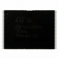
M29W128GH70N6E NUMONYX, M29W128GH70N6E Datasheet - Page 54

M29W128GH70N6E
Manufacturer Part Number
M29W128GH70N6E
Description
IC FLASH 128MBIT 70NS 56TSOP
Manufacturer
NUMONYX
Series
Axcell™r
Datasheet
1.M29W128GH70N6E.pdf
(94 pages)
Specifications of M29W128GH70N6E
Format - Memory
FLASH
Memory Type
FLASH
Memory Size
128M (16Mx8, 8Mx16)
Speed
70ns
Interface
Parallel
Voltage - Supply
2.7 V ~ 3.6 V
Operating Temperature
-40°C ~ 85°C
Package / Case
56-TSOP
Package
56TSOP
Cell Type
NOR
Density
128 Mb
Architecture
Sectored
Block Organization
Symmetrical
Typical Operating Supply Voltage
3|3.3 V
Sector Size
128KByte x 128
Timing Type
Asynchronous
Interface Type
Parallel
Lead Free Status / RoHS Status
Lead free / RoHS Compliant
Available stocks
Company
Part Number
Manufacturer
Quantity
Price
Company:
Part Number:
M29W128GH70N6E
Manufacturer:
Numonyx
Quantity:
17 280
Company:
Part Number:
M29W128GH70N6E
Manufacturer:
MICRON
Quantity:
595
Company:
Part Number:
M29W128GH70N6E
Manufacturer:
MICRON45
Quantity:
556
Part Number:
M29W128GH70N6E
Manufacturer:
ST
Quantity:
20 000
7.2.4
7.2.5
7.3
54/94
before other commands are issued. The error bit is output on DQ5 when the status register
is read.
Note that the Program command cannot change a bit set to ’0’ back to ’1’ and attempting to
do so will set DQ5 to ‘1’. A bus read operation to that address will show the bit is still ‘0’. One
of the erase commands must be used to set all the bits in a block or in the whole memory
from ’0’ to ’1’.
Erase timer bit (DQ3)
The erase timer bit can be used to identify the start of program/erase controller operation
during a Block Erase command. Once the program/erase controller starts erasing the erase
timer bit is set to ’1’. Before the program/erase controller starts the erase timer bit is set to ’0’
and additional blocks to be erased may be written to the command interface. The erase
timer bit is output on DQ3 when the status register is read.
Alternative toggle bit (DQ2)
The alternative toggle bit can be used to monitor the program/erase controller during erase
operations. The alternative toggle bit is output on DQ2 when the status register is read.
During chip erase and block erase operations the toggle bit changes from ’0’ to ’1’ to ’0’,
etc., with successive bus read operations from addresses within the blocks being erased. A
protected block is treated the same as a block not being erased. Once the operation
completes the memory returns to read mode.
During erase suspend the alternative toggle bit changes from ’0’ to ’1’ to ’0’, etc. with
successive bus read operations from addresses within the blocks being erased. Bus read
operations to addresses within blocks not being erased will output the memory array data as
if in read mode.
After an erase operation that causes the error bit to be set, the alternative toggle bit can be
used to identify which block or blocks have caused the error. The alternative toggle bit
changes from ’0’ to ’1’ to ’0’, etc. with successive bus read operations from addresses within
blocks that have not erased correctly. The alternative toggle bit does not change if the
addressed block has erased correctly.
Buffered program abort bit (DQ1)
The buffered program abort bit, DQ1, is set to ‘1’ when a write to buffer program or
enhanced buffered program operation aborts. The Buffered Program Abort and Reset
command must be issued to return the device to read mode (see write to buffer program in
Section 6.1: Standard
commands).


