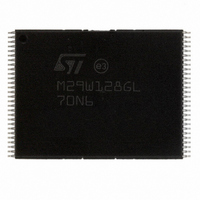
M29W128GL70N6E NUMONYX, M29W128GL70N6E Datasheet - Page 40

M29W128GL70N6E
Manufacturer Part Number
M29W128GL70N6E
Description
IC FLASH 128MBIT 70NS 56TSOP
Manufacturer
NUMONYX
Series
Axcell™r
Datasheet
1.M29W128GH70N6E.pdf
(94 pages)
Specifications of M29W128GL70N6E
Format - Memory
FLASH
Memory Type
FLASH
Memory Size
128M (16Mx8, 8Mx16)
Speed
70ns
Interface
Parallel
Voltage - Supply
2.7 V ~ 3.6 V
Operating Temperature
-40°C ~ 85°C
Package / Case
56-TSOP
Package
56TSOP
Cell Type
NOR
Density
128 Mb
Architecture
Sectored
Block Organization
Symmetrical
Typical Operating Supply Voltage
3|3.3 V
Sector Size
128KByte x 128
Timing Type
Asynchronous
Interface Type
Parallel
Lead Free Status / RoHS Status
Lead free / RoHS Compliant
Available stocks
Company
Part Number
Manufacturer
Quantity
Price
Company:
Part Number:
M29W128GL70N6E
Manufacturer:
MICRON
Quantity:
11 200
Company:
Part Number:
M29W128GL70N6E
Manufacturer:
LATTICE
Quantity:
198
Part Number:
M29W128GL70N6E
Manufacturer:
MICRON
Quantity:
20 000
Table 13.
1. X don’t care, PA program address, PD program data, BAd any address in the block, WBL write buffer location. All values in
2. The maximum number of cycles in the command sequence is 36. N+1 is the number of words to be programmed during
3. Each buffer has the same A22-A5 addresses. A0-A4 are used to select a word within the N+1 word page.
4. The 6th cycle has to be issued N time. WBL scans the word inside the page.
5. BAd must be identical to the address loaded during the write to buffer program 3rd and 4th cycles.
Table 14.
1. Only available from week 8 of 2008.
40/94
Write to Buffer
Program
Write to Buffer
Program Confirm
Buffered Program
Abort and Reset
Unlock Bypass
Unlock Bypass
Program
Unlock Bypass
Block Erase
Unlock Bypass
Chip Erase
Unlock Bypass
Write to Buffer
Program
Unlock Bypass
Reset
Enhanced
Buffered
Program
Enhanced
Buffered
Program
Confirm
Unlock
Bypass
Enhanced
Buffered
Program
Command
the table are in hexadecimal.
the write to buffer program operation.
Command
259
257 BAd
1
Fast program commands, 16-bit mode
Enhanced buffered program commands, 16-bit mode
Add
BAd
555
(00)
1st
Data
N+5
N+3
AA
29
33
2+
1
3
3
2
2
2
Add Data Add Data Add Data
2AA
BAd
(00)
Add
BAd
BAd
555
555
555
(5)
X
X
X
X
2nd
Data
1st
55
Data
AA
AA
AA
A0
29
80
80
25
90
BAd
3rd
Add
2AA
2AA
2AA
BAd
BAd
33
PA
X
X
2nd
BAd
(00)
Data
N
PD
55
55
55
30
10
00
4th
(2)
Data
Bus write operations
Add
BAd
555
555
PA
(3)
Bus write operations
Add
...
3rd
...
Data
Data
PD
25
F0
20
...
Add
BAd
(FF)
WBL
Add
BAd
257th
(6)
4th
Data
Data
(1)
Data
N
PD
(2)
(1)
Add
258th
PA
Add
Data
(3)
5th
Add
BAd
(FF)
Data
PD
259th
Data
Data
WBL
Add
(4)
Add
6th
260th
Data
PD
Data


