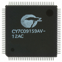
CY7C09159AV-12AC Cypress Semiconductor Corp, CY7C09159AV-12AC Datasheet - Page 2

CY7C09159AV-12AC
Manufacturer Part Number
CY7C09159AV-12AC
Description
IC SRAM 72KBIT 12NS 100LQFP
Manufacturer
Cypress Semiconductor Corp
Datasheet
1.CY7C09159AV-12AC.pdf
(17 pages)
Specifications of CY7C09159AV-12AC
Format - Memory
RAM
Memory Type
SRAM - Dual Port, Synchronous
Memory Size
72K (8K x 9)
Speed
12ns
Interface
Parallel
Voltage - Supply
3 V ~ 3.6 V
Operating Temperature
0°C ~ 70°C
Package / Case
100-LQFP
Lead Free Status / RoHS Status
Contains lead / RoHS non-compliant
Other names
428-1177
Available stocks
Company
Part Number
Manufacturer
Quantity
Price
Company:
Part Number:
CY7C09159AV-12AC
Manufacturer:
CYPRESS
Quantity:
150
Company:
Part Number:
CY7C09159AV-12AC
Manufacturer:
Cypress Semiconductor Corp
Quantity:
10 000
Functional Description
The CY7C09159AV and CY7C09169AV are high-speed syn-
chronous CMOS 8K and 16K x 9 dual-port static RAMs. Two
ports are provided, permitting independent, simultaneous ac-
cess for reads and writes to any location in memory.
ters on control, address, and data lines allow for minimal set-
up and hold times. In pipelined output mode, data is registered
for decreased cycle time. Clock to data valid t
lined). Flow-through mode can also be used to bypass the
pipelined output register to eliminate access latency. In flow-
through mode data will be available t
address is clocked into the device. Pipelined output or flow-
through mode is selected via the FT/Pipe pin.
Each port contains a burst counter on the input address regis-
ter. The internal write pulse width is independent of the LOW-
to-HIGH transition of the clock signal. The internal write pulse
is self-timed to allow the shortest possible cycle times.
Note:
Document #: 38-06053 Rev. *A
2.
When simultaneously writing to the same location, final value cannot be guaranteed.
CD1
= 18 ns after the
CD2
= 9 ns (pipe-
[2]
Regis-
A HIGH on CE
down the internal circuitry to reduce the static power consump-
tion. The use of multiple Chip Enables allows easier banking
of multiple chips for depth expansion configurations. In the
pipelined mode, one cycle is required with CE
HIGH to reactivate the outputs.
Counter enable inputs are provided to stall the operation of the
address input and utilize the internal address generated by the
internal counter for fast interleaved memory applications. A
port’s burst counter is loaded with the port’s Address Strobe
(ADS). When the port’s Count Enable (CNTEN) is asserted,
the address counter will increment on each LOW-to-HIGH
transition of that port’s clock signal. This will read/write one
word from/into each successive address location until CNTEN
is deasserted. The counter can address the entire memory
array and will loop back to the start. Counter Reset (CNTRST)
is used to reset the burst counter.
All parts are available in 100-pin Thin Quad Plastic Flatpack
(TQFP) packages.
0
or LOW on CE
1
for one clock cycle will power
CY7C09159AV
CY7C09169AV
0
LOW and CE
Page 2 of 17
1


