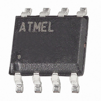
AT25040N-10SI Atmel, AT25040N-10SI Datasheet - Page 8

AT25040N-10SI
Manufacturer Part Number
AT25040N-10SI
Description
IC EEPROM 4KBIT 2.1MHZ 8SOIC
Manufacturer
Atmel
Datasheet
1.AT25010-10PC.pdf
(17 pages)
Specifications of AT25040N-10SI
Format - Memory
EEPROMs - Serial
Memory Type
EEPROM
Memory Size
4K (512 x 8)
Speed
2.1MHz
Interface
SPI, 3-Wire Serial
Voltage - Supply
4.5 V ~ 5.5 V
Operating Temperature
-40°C ~ 85°C
Package / Case
8-SOIC (3.9mm Width)
Lead Free Status / RoHS Status
Contains lead / RoHS non-compliant
Available stocks
Company
Part Number
Manufacturer
Quantity
Price
Company:
Part Number:
AT25040N-10SI-2.7
Manufacturer:
HITACHI
Quantity:
880
Part Number:
AT25040N-10SI-2.7
Manufacturer:
ATMEL/爱特梅尔
Quantity:
20 000
READ SEQUENCE (READ): Reading the AT25010/020/040 via the SO (Serial Output)
pin requires the following sequence. After the CS line is pulled low to select a device,
the READ op-code (including A8) is transmitted via the SI line followed by the byte
address to be read (A7-A0). Upon completion, any data on the SI line will be ignored.
The data (D7-D0) at the specified address is then shifted out onto the SO line. If only
one byte is to be read, the CS line should be driven high after the data comes out. The
READ sequence can be continued since the byte address is automatically incremented
and data will continue to be shifted out. When the highest address is reached, the
address counter will roll over to the lowest address allowing the entire memory to be
read in one continuous READ cycle.
WRITE SEQUENCE (WRITE): In order to program the AT25010/020/040, the Write
Protect pin (WP) must be held high and two separate instructions must be executed.
First, the device must be write enabled via the Write Enable (WREN) Instruction. Then
a Write (WRITE) Instruction may be executed. Also, the address of the memory loca-
tion(s) to be programmed must be outside the protected address field location selected
by the Block Write Protection Level. During an internal write cycle, all commands will be
ignored except the RDSR instruction.
A Write Instruction requires the following sequence. After the CS line is pulled low to
select the device, the WRITE op-code (including A8) is transmitted via the SI line fol-
lowed by the byte address (A7-A0) and the data (D7-D0) to be programmed.
Programming will start after the CS pin is brought high. (The LOW to High transition of
the CS pin must occur during the SCK low time immediately after clocking in the D0
(LSB) data bit.
The READY/BUSY status of the device can be determined by initiating a READ STA-
TUS REGISTER (RDSR) Instruction. If Bit 0 = 1, the WRITE cycle is still in progress. If
Bit 0 = 0, the WRITE cycle has ended. Only the READ STATUS REGISTER instruction
is enabled during the WRITE programming cycle.
The AT25010/020/040 is capable of an 8-byte PAGE WRITE operation. After each byte
of data is received, the three low order address bits are internally incremented by one;
the six high order bits of the address will remain constant. If more than 8 bytes of data
are transmitted, the address counter will roll over and the previously written data will be
overwritten. The AT25010/020/040 is automatically returned to the write disable state at
the completion of a WRITE cycle.
NOTE: If the WP pin is brought low or if the device is not Write enabled (WREN), the
device will ignore the Write instruction and will return to the standby state, when CS is
brought high. A new CS falling edge is required to re-initiate the serial communication.
AT25010/020/040
8
0606M–SEEPR–06/03


