AT28BV256-20SI Atmel, AT28BV256-20SI Datasheet - Page 4
AT28BV256-20SI
Manufacturer Part Number
AT28BV256-20SI
Description
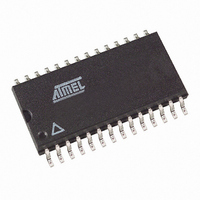
IC EEPROM 256KBIT 200NS 28SOIC
Manufacturer
Atmel
Datasheet
1.AT28BV256-20SU.pdf
(17 pages)
Specifications of AT28BV256-20SI
Format - Memory
EEPROMs - Parallel
Memory Type
EEPROM
Memory Size
256K (32K x 8)
Speed
200ns
Interface
Parallel
Voltage - Supply
2.7 V ~ 3.6 V
Operating Temperature
-40°C ~ 85°C
Package / Case
28-SOIC (7.5mm Width)
Lead Free Status / RoHS Status
Contains lead / RoHS non-compliant
Available stocks
Company
Part Number
Manufacturer
Quantity
Price
Company:

Part Number:
AT28BV256-20SI
Manufacturer:
ATM
Quantity:
3 000


5. Device Operation
5.1
5.2
5.3
5.4
5.5
5.6
4
Read
Byte Write
Page Write
Data Polling
Toggle Bit
Data Protection
AT28BV256
The AT28BV256 is accessed like a Static RAM. When CE and OE are low and WE is high, the
data stored at the memory location determined by the address pins is asserted on the outputs.
The outputs are put in the high impedance state when either CE or OE is high. This dual-line
control gives designers flexibility in preventing bus contention in their system.
A low pulse on the WE or CE input with CE or WE low (respectively) and OE high initiates a write
cycle. The address is latched on the falling edge of CE or WE, whichever occurs last. The data is
latched by the first rising edge of CE or WE. Once a byte write has been started, it will automati-
cally time itself to completion. Once a programming operation has been initiated and for the
duration of t
The page write operation of the AT28BV256 allows 1 to 64 bytes of data to be written into the
device during a single internal programming period. A page write operation is initiated in the
same manner as a byte write; the first byte written can then be followed by 1 to 63 additional
bytes. Each successive byte must be written within 150 µs (t
limit is exceeded the AT28BV256 will cease accepting data and commence the internal pro-
gramming operation. All bytes during a page write operation must reside on the same page as
defined by the state of the A6 - A14 inputs. For each WE high to low transition during the page
write operation, A6 - A14 must be the same.
The A0 to A5 inputs are used to specify which bytes within the page are to be written. The bytes
may be loaded in any order and may be altered within the same load period. Only bytes which
are specified for writing will be written; unnecessary cycling of other bytes within the page does
not occur.
The AT28BV256 features Data Polling to indicate the end of a write cycle. During a byte or page
write cycle, an attempted read of the last byte written will result in the complement of the written
data to be presented on I/O7. Once the write cycle has been completed, true data is valid on all
outputs, and the next write cycle may begin. Data Polling may begin at anytime during the write
cycle.
In addition to Data Polling, the AT28BV256 provides another method for determining the end of
a write cycle. During the write operation, successive attempts to read data from the device will
result in I/O6 toggling between one and zero. Once the write has completed, I/O6 will stop tog-
gling and valid data will be read. Reading the toggle bit may begin at any time during the write
cycle.
If precautions are not taken, inadvertent writes may occur during transitions of the host system
power supply. Atmel
memory against inadvertent writes.
WC
, a read operation will effectively be a polling operation.
®
has incorporated both hardware and software features that will protect the
BLC
) of the previous byte. If the t
0273K–PEEPR–2/09
BLC
Related parts for AT28BV256-20SI
Image
Part Number
Description
Manufacturer
Datasheet
Request
R

Part Number:
Description:
IC EEPROM 256KBIT 200NS 28SOIC
Manufacturer:
Atmel
Datasheet:

Part Number:
Description:
IC EEPROM 256KBIT 200NS 28TSOP
Manufacturer:
Atmel
Datasheet:

Part Number:
Description:
IC EEPROM 256KBIT 200NS 32PLCC
Manufacturer:
Atmel
Datasheet:
Part Number:
Description:
IC EEPROM 256KBIT 200NS 32PLCC
Manufacturer:
Atmel
Datasheet:
Part Number:
Description:
IC EEPROM 256KBIT 200NS 32PLCC
Manufacturer:
Atmel
Datasheet:
Part Number:
Description:
IC EEPROM 256KBIT 200NS 28TSOP
Manufacturer:
Atmel
Datasheet:

Part Number:
Description:
256k 32k X 8 Battery-voltage Parallel Eeproms
Manufacturer:
ATMEL Corporation
Datasheet:

Part Number:
Description:
IC EEPROM 256KBIT 200NS 28DIP
Manufacturer:
Atmel
Datasheet:
Part Number:
Description:
IC EEPROM 256KBIT 200NS 28DIP
Manufacturer:
Atmel
Datasheet:
Part Number:
Description:
IC EEPROM 256KBIT 200NS 28SOIC
Manufacturer:
Atmel
Datasheet:
Part Number:
Description:
IC EEPROM 256KBIT 200NS 28TSOP
Manufacturer:
Atmel
Datasheet:
Part Number:
Description:
IC EEPROM 256KBIT 200NS 32PLCC
Manufacturer:
Atmel
Datasheet:
Part Number:
Description:
IC EEPROM 256KBIT 200NS 28SOIC
Manufacturer:
Atmel
Datasheet:
Part Number:
Description:
IC EEPROM 256KBIT 200NS 28TSOP
Manufacturer:
Atmel
Datasheet: