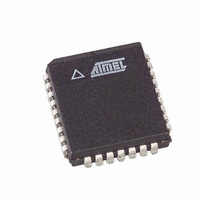
AT49LH004-33JC SL383 Atmel, AT49LH004-33JC SL383 Datasheet - Page 19

AT49LH004-33JC SL383
Manufacturer Part Number
AT49LH004-33JC SL383
Description
IC FLASH 4MBIT 33MHZ 32PLCC
Manufacturer
Atmel
Datasheet
1.AT49LH004-33JC.pdf
(40 pages)
Specifications of AT49LH004-33JC SL383
Format - Memory
FLASH
Memory Type
FLASH
Memory Size
4M (512K x 8)
Speed
33MHz
Interface
Parallel
Voltage - Supply
3 V ~ 3.6 V
Operating Temperature
0°C ~ 85°C
Package / Case
32-PLCC
Lead Free Status / RoHS Status
Contains lead / RoHS non-compliant
11.2
3383D–FLASH–6/05
Register-Based Sector Locking
The TBL and WP pins function independently from the Sector Locking Registers. These pins,
when active, will write protect the appropriate sector(s) against program and erase operations
regardless of the values of the Sector Locking Registers. For example, when TBL is active,
writing to the top sector is prevented regardless of the state of the Write-Lock bit for the top
sector’s locking register. In such a case, clearing the Write-Lock bit in the Sector Locking Reg-
ister will have no functional effect even though the register may indicate that the sector is no
longer locked. However, the register may still be set to Read-Lock the sector if desired.
For protecting the sectors of the memory array, the TBL and WP pins always take precedence
over the Sector Locking Registers. In addition, the states of the TBL and WP pins have no
effect on the values or status of the Sector Locking Registers.
The device has eight Sector Locking Registers in FWH mode and 11 Sector Locking Registers
in LPC mode that are used in lieu of or in conjunction with the TBL and WP pins to control the
lock protection for each sector in the memory array. The Sector Locking Registers are
accessed through their respective address locations (detailed in
tem memory map. Since the address bit used to distinguish between memory and register
accesses differs when the device is used as a FWH or LPC Flash (A22 for FWH and A23 for
LPC), the register memory address will also differ.
The Sector Locking Registers are both readable and writable, and each register has three
dedicated locking bits to control Read Lock, Write Lock, and Lock Down functions. Therefore,
a Sector Locking Register can be read to determine what its current value is set to (e.g., set to
Lock Down status). Reading the Sector Locking Registers, however, will not determine the
status of the TBL and WP pins.
When returning from a reset condition or after power-up, the Sector Locking Registers will
always default to a state of 01H.
Table 11-2.
Note:
S10_LK
Register
S9_LK
S8_LK
S7_LK
S6_LK
S5_LK
S4_LK
S3_LK
S2_LK
S1_LK
S0_LK
Name
1. In FWH mode, these registers are treated as one; therefore, only one Sector Locking Regis-
(1)
(1)
(1)
(1)
ter is available for all sub-sectors (sectors 10, 9, 8, and 7) and the sub-sectors cannot be
individually protected. The default value for this register is 01H.
Sector Locking Registers
Associated
Sector
10
9
8
7
6
5
4
3
2
1
0
Sector Size
(Bytes)
32K
16K
64K
64K
64K
64K
64K
64K
64K
8K
8K
FWH MODE
FFBD0002H
FFBC0002H
FFBF0002H
FFBE0002H
FFBB0002H
FFBA0002H
FFB90002H
FFB80002H
Register Memory Address
FF7E0002H
FF7D0002H
FF7C0002H
FF7B0002H
FF7A0002H
LPC MODE
FF7F8002H
FF7F6002H
FF7F4002H
FF7F0002H
FF790002H
FF780002H
Table
11-2) in the 4 GB sys-
AT49LH004
Default Value
01H
01H
01H
01H
01H
01H
01H
01H
01H
01H
01H
19


