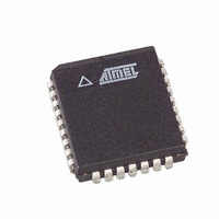
AT49LH004-33JC SL383 Atmel, AT49LH004-33JC SL383 Datasheet - Page 7

AT49LH004-33JC SL383
Manufacturer Part Number
AT49LH004-33JC SL383
Description
IC FLASH 4MBIT 33MHZ 32PLCC
Manufacturer
Atmel
Datasheet
1.AT49LH004-33JC.pdf
(40 pages)
Specifications of AT49LH004-33JC SL383
Format - Memory
FLASH
Memory Type
FLASH
Memory Size
4M (512K x 8)
Speed
33MHz
Interface
Parallel
Voltage - Supply
3 V ~ 3.6 V
Operating Temperature
0°C ~ 85°C
Package / Case
32-PLCC
Lead Free Status / RoHS Status
Contains lead / RoHS non-compliant
7.1
7.2
3383D–FLASH–6/05
FWH4/LFRAME Pin
FWH/LAD[3:0] Pins
Since the AT49LH004 can be used as either a FWH Flash or an LPC Flash, the device
is capable of automatically detecting which type of memory cycle is being performed. For a
FWH/LPC cycle, the host will drive the FWH4/LFRAME pin low for one or more clock cycles to
initiate the operation. After driving the FWH4/LFRAME pin low, the host will send a
START value to indicate the type of FWH/LPC cycle that is to be performed. The value of the
START field determines whether the device will operate using a FWH cycle or an LPC cycle.
Table 7-1
Table 7-1.
If a valid START value is not detected, then the device will enter standby mode when the
FWH4/LFRAME pin is high and no internal operation is in progress. The FWH/LAD[3:0] pins
will also be placed in a high-impedance state.
FWH4/LFRAME is used by the master to indicate the start of cycles and the termination of
cycles due to an abort or time-out condition. This signal is to be used by peripherals to know
when to monitor the bus for a cycle.
The FWH4/LFRAME signal is used as a general notification that the FWH/LAD[3:0] lines con-
tain information relative to the start or stop of a cycle, and that peripherals must monitor the
bus to determine whether the cycle is intended for them. The benefit to peripherals of
FWH4/LFRAME is that it allows them to enter lower power states internally when a cycle is not
intended for them.
When peripherals sample FWH4/LFRAME is active, they are to immediately stop driving the
FWH/LAD[3:0] signal lines on the next clock and monitor the bus for new cycle information.
The FWH/LAD[3:0] signal lines communicate address, control, and data information over the
LPC bus between a master and a peripheral. The information communicated are: start, stop
(abort a cycle), transfer type (memory, I/O, DMA), transfer direction (read/write), address,
data, wait states, DMA channel, and bus master grant.
START Value
0000b
1101b
1110b
details the three valid START fields that the device will recognize.
FWH/LPC Start Fields
Cycle Type
LPC Cycle – The type (memory, I/O, DMA) and direction of the cycle (read or write)
is determined by the second field (CYCTYPE + DIR) of the LPC cycle. Only memory
cycles are supported by the device.
FWH Memory Read Cycle
FWH Memory Write Cycle
AT49LH004
7


