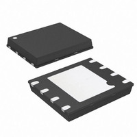
AT45DB041D-MU-2.5 Atmel, AT45DB041D-MU-2.5 Datasheet - Page 17

AT45DB041D-MU-2.5
Manufacturer Part Number
AT45DB041D-MU-2.5
Description
IC FLASH 4MBIT 66MHZ 8MLF
Manufacturer
Atmel
Datasheet
1.AT45DB041D-MU.pdf
(55 pages)
Specifications of AT45DB041D-MU-2.5
Format - Memory
FLASH
Memory Type
DataFLASH
Memory Size
4M (2048 pages x 264 bytes)
Speed
66MHz
Interface
SPI, RapidS
Voltage - Supply
2.5 V ~ 3.6 V
Operating Temperature
-40°C ~ 85°C
Package / Case
8-VFQFN, 8-VFQFPN
Architecture
Sectored
Interface Type
SPI
Supply Voltage (max)
3.6 V
Supply Voltage (min)
2.5 V
Maximum Operating Current
15 mA
Mounting Style
SMD/SMT
Organization
64 KB x 8
Density
4Mb
Access Time (max)
8ns
Boot Type
Not Required
Address Bus
1b
Operating Supply Voltage (typ)
3/3.3V
Operating Temp Range
-40C to 85C
Package Type
MLF
Program/erase Volt (typ)
2.5 to 3.6V
Sync/async
Synchronous
Operating Temperature Classification
Industrial
Operating Supply Voltage (min)
2.5V
Operating Supply Voltage (max)
3.6V
Supply Current
15mA
Mounting
Surface Mount
Pin Count
8
Lead Free Status / RoHS Status
Lead free / RoHS Compliant
Available stocks
Company
Part Number
Manufacturer
Quantity
Price
Company:
Part Number:
AT45DB041D-MU-2.5
Manufacturer:
ATMEL
Quantity:
1 600
Part Number:
AT45DB041D-MU-2.5
Manufacturer:
ATMEL/爱特梅尔
Quantity:
20 000
9.1.3
9.1.4
3595P–DFLASH–09/09
Read Sector Protection Register Command
Various Aspects About the Sector Protection Register
To read the Sector Protection Register, the CS pin must first be asserted. Once the CS pin has
been asserted, an opcode of 32H and 3 dummy bytes must be clocked in via the SI pin. After the
last bit of the opcode and dummy bytes have been clocked in, any additional clock pulses on the
SCK pins will result in data for the content of the Sector Protection Register being output on the
SO pin. The first byte corresponds to sector 0 (0a, 0b), the second byte corresponds to sector 1
and the last byte (byte 8) corresponds to sector 7. Once the last byte of the Sector Protection
Register has been clocked out, any additional clock pulses will result in undefined data being
output on the SO pin. The CS must be deasserted to terminate the Read Sector Protection Reg-
ister operation and put the output into a high-impedance state.
Note:
Figure 9-4.
The Sector Protection Register is subject to a limit of 10,000 erase/program cycles. Users are
encouraged to carefully evaluate the number of times the Sector Protection Register will be
modified during the course of the applications’ life cycle. If the application requires that the Sec-
tor Protection Register be modified more than the specified limit of 10,000 cycles because the
application needs to temporarily unprotect individual sectors (sector protection remains enabled
while the Sector Protection Register is reprogrammed), then the application will need to limit this
practice. Instead, a combination of temporarily unprotecting individual sectors along with dis-
abling sector protection completely will need to be implemented by the application to ensure that
the limit of 10,000 cycles is not exceeded.
CS
SO
Command
Read Sector Protection Register
SI
Each transition
represents 8 bits
xx = Dummy Byte
Read Sector Protection Register
Opcode
X
X
Byte 1
32H
X
Data Byte
Byte 2
n
xxH
Data Byte
n + 1
AT45DB041D
Byte 3
xxH
Data Byte
n + 7
Byte 4
xxH
17


