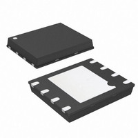
AT45DB041D-MU-2.5 Atmel, AT45DB041D-MU-2.5 Datasheet - Page 23

AT45DB041D-MU-2.5
Manufacturer Part Number
AT45DB041D-MU-2.5
Description
IC FLASH 4MBIT 66MHZ 8MLF
Manufacturer
Atmel
Datasheet
1.AT45DB041D-MU.pdf
(55 pages)
Specifications of AT45DB041D-MU-2.5
Format - Memory
FLASH
Memory Type
DataFLASH
Memory Size
4M (2048 pages x 264 bytes)
Speed
66MHz
Interface
SPI, RapidS
Voltage - Supply
2.5 V ~ 3.6 V
Operating Temperature
-40°C ~ 85°C
Package / Case
8-VFQFN, 8-VFQFPN
Architecture
Sectored
Interface Type
SPI
Supply Voltage (max)
3.6 V
Supply Voltage (min)
2.5 V
Maximum Operating Current
15 mA
Mounting Style
SMD/SMT
Organization
64 KB x 8
Density
4Mb
Access Time (max)
8ns
Boot Type
Not Required
Address Bus
1b
Operating Supply Voltage (typ)
3/3.3V
Operating Temp Range
-40C to 85C
Package Type
MLF
Program/erase Volt (typ)
2.5 to 3.6V
Sync/async
Synchronous
Operating Temperature Classification
Industrial
Operating Supply Voltage (min)
2.5V
Operating Supply Voltage (max)
3.6V
Supply Current
15mA
Mounting
Surface Mount
Pin Count
8
Lead Free Status / RoHS Status
Lead free / RoHS Compliant
Available stocks
Company
Part Number
Manufacturer
Quantity
Price
Company:
Part Number:
AT45DB041D-MU-2.5
Manufacturer:
ATMEL
Quantity:
1 600
Part Number:
AT45DB041D-MU-2.5
Manufacturer:
ATMEL/爱特梅尔
Quantity:
20 000
AT45DB041D
The result of the most recent Main Memory Page to Buffer Compare operation is indicated using
bit 6 of the status register. If bit 6 is a 0, then the data in the main memory page matches the
data in the buffer. If bit 6 is a 1, then at least one bit of the data in the main memory page does
not match the data in the buffer.
Bit 1 in the Status Register is used to provide information to the user whether or not the sector
protection has been enabled or disabled, either by software-controlled method or hardware-con-
trolled method. A logic 1 indicates that sector protection has been enabled and logic 0 indicates
that sector protection has been disabled.
Bit 0 in the Status Register indicates whether the page size of the main memory array is config-
ured for “power of 2” binary page size (256 bytes) or the DataFlash standard page size
(264 bytes). If bit 0 is a 1, then the page size is set to 256 bytes. If bit 0 is a 0, then the page size
is set to 264 bytes.
The device density is indicated using bits 5, 4, 3, and 2 of the status register. For the
AT45DB041D, the four bits are 0111 The decimal value of these four binary bits does not equate
to the device density; the four bits represent a combinational code relating to differing densities
of DataFlash devices. The device density is not the same as the density code indicated in the
JEDEC device ID information. The device density is provided only for backward compatibility.
Table 11-1.
Status Register Format
Bit 7
Bit 6
Bit 5
Bit 4
Bit 3
Bit 2
Bit 1
Bit 0
RDY/BUSY
COMP
0
1
1
1
PROTECT
PAGE SIZE
23
3595P–DFLASH–09/09


