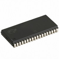
CY7C1049B-15VXC Cypress Semiconductor Corp, CY7C1049B-15VXC Datasheet

CY7C1049B-15VXC
Specifications of CY7C1049B-15VXC
Related parts for CY7C1049B-15VXC
CY7C1049B-15VXC Summary of contents
Page 1
... For guidelines on SRAM system design, please refer to the ‘System Design Guidelines’ Cypress application note, available on the internet at www.cypress.com. Cypress Semiconductor Corporation Document #: 38-05169 Rev. *B Functional Description The CY7C1049B is a high-performance CMOS static RAM organized as 524,288 words by 8 bits. Easy memory expansion is provided by an active LOW Chip Enable (CE), an active LOW Output Enable (OE), and tri-state drivers. Writing to the device is accomplished by taking Chip Enable (CE) and Write Enable (WE) inputs LOW ...
Page 2
... MAX > > < MAX , Com’l CC – 0.3V, CC Com’l L > V – 0.3V < 0.3V Ind’l IN CY7C1049B -12 - 240 220 Ambient Temperature 0°C to +70°C 4.5V–5.5V –40°C to +85°C -12 -15 -17 Max. Min. Max. Min. 2.4 2.4 0.4 0 ...
Page 3
... Tested initially and after any design or process changes that may affect these parameters. Document #: 38-05169 Rev. *B Test Conditions T = 25° MHz 5. 481 Ω 5V 3.0V R2 GND 5 pF 255Ω INCLUDING JIG AND SCOPE (b) 1.73V CY7C1049B Max ALL INPUT PULSES 90% 10% ≤ Page Unit pF pF 90% 10% ≤ ...
Page 4
... No input may exceed V + 0.5V. CC Document #: 38-05169 Rev. *B [4] -12 Min. Max. [ Over the Operating Range Com’ > > power is less than less than t , and t HZCE LZCE HZOE LZOE HZWE CY7C1049B -15 -17 Min. Max. Min. Max [11] Conditions Min. Max. ...
Page 5
... Notes: 12. Device is continuously selected HIGH for read cycle. 14. Address valid prior to or coincident with CE transition LOW. Document #: 38-05169 Rev. *B DATA RETENTION MODE 3.0V V > CDR OHA ACE t DOE t LZOE 50 CY7C1049B 3. DATA VALID t HZOE t HZCE IMPEDANCE DATA VALID t PD 50% HIGH Page ...
Page 6
... If CE goes HIGH simultaneously with WE going HIGH, the output remains in a high-impedance state. 17. During this period the I/Os are in the output state and input signals should not be applied. Document #: 38-05169 Rev SCE SCE PWE t SD DATA VALID [15, 16 SCE PWE t SD DATA VALID IN CY7C1049B Page ...
Page 7
... Switching Waveforms (continued) Write Cycle No. 3 (WE Controlled, OE LOW) ADDRESS NOTE 17 DATA I/O Ordering Information Speed (ns) Ordering Code 12 CY7C1049B-12VC CY7C1049B-12VXC 15 CY7C1049B-15VC CY7C1049B-15VXC CY7C1049B-15VI CY7C1049B-15VXI 17 CY7C1049BL-17VC Document #: 38-05169 Rev. *B [16 SCE PWE t HZWE Package Name 51-85090 36-Lead (400-Mil) Molded SOJ 36-Lead (400-Mil) Molded SOJ (Pb-free) ...
Page 8
... The inclusion of Cypress products in life-support systems application implies that the manufacturer assumes all risk of such use and in doing so indemnifies Cypress against all charges. CY7C1049B 51-85090-*B ...
Page 9
... Document History Page Document Title: CY7C1049B 512K x 8 Static RAM Document Number: 38-05169 Issue REV. ECN NO. Date ** 110209 12/02/01 *A 116465 09/16/02 *B 498501 See ECN Document #: 38-05169 Rev. *B Orig. of Change SZV Change from Spec number: 38-00937 to 38-05169 CEA Add applications foot note to data sheet, page 1 ...


