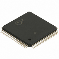
CY7C09199V-12AXC Cypress Semiconductor Corp, CY7C09199V-12AXC Datasheet

CY7C09199V-12AXC
Specifications of CY7C09199V-12AXC
Available stocks
Related parts for CY7C09199V-12AXC
CY7C09199V-12AXC Summary of contents
Page 1
... A –A for 64K, and A – Cypress Semiconductor Corporation Document #: 38-06043 Rev. *C 3.3V 32K/64K/128K x 8/9 Synchronous Dual-Port Static RAM High speed clock to data access 6.5[1]/7.5[1]/9/12 ns (max.) ■ 3.3V low operating power ■ Active= 115 mA (typical) ■ Standby= 10 μA (typical) ■ ...
Page 2
... CD1 that port’s clock signal. This reads/writes one word from/into each successive address location until CNTEN is deasserted. The counter can address the entire memory array and loops back to the start. Counter Reset (CNTRST) is used to reset the burst counter. All parts are available in 100-pin Thin Quad Plastic Flatpack (TQFP) packages ...
Page 3
... Pin Configurations (continued Figure 2. 100-Pin TQFP (Top View0 - CY7C09199V (128K x 9), CY7C09189V (64K x 9),CY7C09179V (32K x 9) 100 A7L 3 A8L 4 A9L 5 A10L 6 A11L 7 A12L 8 A13L 9 A14L 10 [8] A15L 11 [9] A16L 12 VCC CE0L 18 CE1L 19 CNTRSTL 20 R/WL 21 OEL 22 FT/PIPEL Document #: 38-06043 Rev CY7C09079V/89V/99V ...
Page 4
... Output Enable Input. This signal must be asserted LOW to enable the I/O data pins during L R read operations. R/W R/W Read/Write Enable Input. This signal is asserted LOW to write to the dual port memory array For read operations, assert this pin HIGH. FT/PIPE Flow-Through/Pipelined Select Input. For flow-through mode operation, assert this pin LOW. ...
Page 5
... IN C Output Capacitance OUT Notes 10. The Voltage on any input or I/O pin cannot exceed the power pin during power-up. 11. Industrial parts are available in CY7C09099V and CY7C09199V only. 12. CE and CE are internal signals. To select either the left or right port, both Document #: 38-06043 Rev. *C Static Discharge Voltage............................................ > ...
Page 6
R1 = 590Ω OUTPUT 435Ω (a) Normal Load (Load 1) Figure 4. AC Test Loads (Applicable to -6 and -7 only 50Ω 50Ω 0 OUTPUT 1.4V ...
Page 7
Switching Characteristics Over the Operating Range Parameter Description f f Flow-Through MAX1 Max f f Pipelined MAX2 Max t Clock Cycle Time - Flow-Through CYC1 t Clock Cycle Time - Pipelined CYC2 t Clock HIGH Time - Flow-Through CH1 t ...
Page 8
Switching Waveforms (continued) Figure 6. Read Cycle for Flow-Through Output (FT/PIPE = CH1 CLK R ADDRESS t CD1 DATA ...
Page 9
Switching Waveforms (continued) Figure 7. Read Cycle for Pipelined Operation (FT/PIPE = V t CYC2 t CH2 CLK R ADDRESS Latency ...
Page 10
Switching Waveforms (continued) Figure 9. Left Port Write to Flow-Through Right Port Read CLK R ADDRESS MATCH VALID DATA INL t CCS CLK R t ...
Page 11
Switching Waveforms (continued) Figure 10. Pipelined Read-to-Write-to-Read ( CYC2 t t CH2 CL2 CLK R ADDRESS DATA IN ...
Page 12
... READ Notes 26. Output state (HIGH, LOW, or high-impedance) is determined by the previous cycle control signals. 27. CE and ADS = CNTEN, and CNTRST = 28. During “No Operation”, data in memory at the selected address may be corrupted and should be re-written to ensure data integrity. Document #: 38-06043 Rev n+1 n+2 ...
Page 13
Switching Waveforms (continued) Figure 12. Flow-Through Read-to-Write-to-Read ( CYC1 t t CH1 CL1 CLK R ADDRESS DATA IN ...
Page 14
Switching Waveforms (continued) Figure 14. Pipelined Read with Address Counter Advance t CYC2 t t CH2 CL2 CLK ADDRESS SAD HAD ADS CNTEN t t SCN HCN DATA OUT Q Q x-1 ...
Page 15
Switching Waveforms (continued) Figure 16. Write with Address Counter Advance (Flow-Through or Pipelined Outputs) t CYC2 t t CH2 CL2 CLK ADDRESS n INTERNAL A n ADDRESS t t SAD HAD ADS CNTEN t t ...
Page 16
Switching Waveforms (continued) Figure 17. Counter Reset (Pipelined Outputs) t CYC2 t t CH2 CL2 CLK ADDRESS INTERNAL A X ADDRESS SAD HAD ADS t t SCN HCN CNTEN t t SRST HRST CNTRST t ...
Page 17
Table 1. Read/Write and Enable Operation Inputs OE CLK Table 2. Address Counter Control Operation Previous Address CLK ADS CNTEN Address ...
Page 18
Ordering Information 32K x8 3.3V Synchronous Dual-Port SRAM Speed (ns) Ordering Code [1] 6.5 CY7C09079V-6AC [1] 7.5 CY7C09079V-7AC CY7C09079V-7AI 9 CY7C09079V-9AC 12 CY7C09079V-12AC 64K x8 3.3V Synchronous Dual-Port SRAM Speed (ns) Ordering Code [1] 6.5 CY7C09089V-6AC CY7C09089V-6AXC [1] 7.5 CY7C09089V-7AC ...
Page 19
... CY7C09199V-7AC CY7C09199V-7AXC 9 CY7C09199V-9AC CY7C09199V-9AXC CY7C09199V-9AI CY7C09199V-9AXI 12 CY7C09199V-12AC CY7C09199V-12AXC Document #: 38-06043 Rev. *C Package Name Package Type A100 100-Pin Thin Quad Flat Pack A100 100-Pin Pb-Free Thin Quad Flat Pack A100 100-Pin Thin Quad Flat Pack A100 100-Pin Thin Quad Flat Pack ...
Page 20
Package Diagram Figure 18. 100-Pin Thin Plastic Quad Flat Pack (TQFP) A100 (51-85048) Document #: 38-06043 Rev. *C CY7C09079V/89V/99V CY7C09179V/89V/99V 51-85048-*B Page [+] Feedback ...
Page 21
... Power up requirements added to Operating Conditions Information Added Pb-Free Logo Added Pb-Free Part Ordering Information: CY7C09089V-6AXC, CY7C09089V-12AXC, CY7C09099V-6AXC, CY7C09099V-7AI, CY7C09099V-7AXI, CY7C09099V-12AXC, CY7C09179V-6AXC, CY7C09179V-12AXC, CY7C09189V-6AXC, CY7C09189V-12AXC, CY7C09199V-6AXC, CY7C09199V-7AXC, CY7C09199V-9AXC, CY7C09199V-9AXI, CY7C09199V-12AXC Added CY7C09089V-12AXI part in the Ordering information table PSoC Solutions psoc.cypress.com General clocks.cypress.com Low Power/Low Voltage ...


