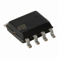
M95010-WMN6P STMicroelectronics, M95010-WMN6P Datasheet - Page 18

M95010-WMN6P
Manufacturer Part Number
M95010-WMN6P
Description
IC EEPROM 1KBIT 10MHZ 8SOIC
Manufacturer
STMicroelectronics
Specifications of M95010-WMN6P
Format - Memory
EEPROMs - Serial
Memory Type
EEPROM
Memory Size
1K (128 x 8)
Speed
10MHz
Interface
SPI, 3-Wire Serial
Voltage - Supply
2.5 V ~ 5.5 V
Operating Temperature
-40°C ~ 85°C
Package / Case
8-SOIC (3.9mm Width)
Memory Configuration
128 X 8
Interface Type
Serial, SPI
Clock Frequency
10MHz
Supply Voltage Range
2.5V To 5.5V
Memory Case Style
SO
No. Of Pins
8
Rohs Compliant
Yes
Lead Free Status / RoHS Status
Lead free / RoHS Compliant
Other names
497-8600-5
M95010-WMN6P
M95010-WMN6P
Available stocks
Company
Part Number
Manufacturer
Quantity
Price
Instructions
6.3
6.3.1
6.3.2
6.3.3
18/43
Read Status Register (RDSR)
One of the major uses of this instruction is to allow the MCU to poll the state of the Write In
Progress (WIP) bit. This is needed because the device will not accept further WRITE or
WRSR instructions when the previous Write cycle is not yet finished.
As shown in
The bits of the instruction byte are then shifted in, on Serial Data Input (D). The current state
of the bits in the Status register is shifted out, on Serial Data Out (Q). The Read Cycle is
terminated by driving Chip Select (S) high.
The Status register may be read at any time, even during a Write cycle (whether it be to the
memory area or to the Status register). All bits of the Status register remain valid, and can
be read using the RDSR instruction. However, during the current Write cycle, the values of
the non-volatile bits (BP0, BP1) become frozen at a constant value. The updated value of
these bits becomes available when a new RDSR instruction is executed, after completion of
the Write cycle. On the other hand, the two read-only bits (Write Enable Latch (WEL), Write
In Progress (WIP)) are dynamically updated during the on-going Write cycle.
Bits b7, b6, b5 and b4 are always read as 1. The status and control bits of the Status
register are as follows:
WIP bit
The Write In Progress (WIP) bit indicates whether the memory is busy with a Write or Write
Status register cycle. When set to 1, such a cycle is in progress, when reset to 0 no such
cycle is in progress.
WEL bit
The Write Enable Latch (WEL) bit indicates the status of the internal Write Enable Latch.
When set to 1 the internal Write Enable Latch is set, when set to 0 the internal Write Enable
Latch is reset and no Write or Write Status Register instruction is accepted.
BP1, BP0 bits
The Block Protect (BP1, BP0) bits are non-volatile. They define the size of the area to be
software protected against Write instructions. These bits are written with the Write Status
Register (WRSR) instruction. When one or both of the Block Protect (BP1, BP0) bits is set to
1, the relevant memory area (as defined in
(WRITE) instructions. The Block Protect (BP1, BP0) bits can be written provided that the
Hardware Protected mode has not been set.
Table 5.
b7
1
Figure
Status register format
1
9, to send this instruction to the device, Chip Select (S) is first driven low.
1
Doc ID 6512 Rev 8
1
Table
3) becomes protected against Write
BP1
Block Protect bits
Write Enable Latch bit
BP0
M95040, M95020, M95010
WEL
Write In Progress bit
WIP
b0


