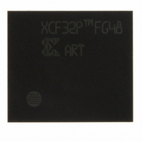
XCF32PFSG48C Xilinx Inc, XCF32PFSG48C Datasheet - Page 4

XCF32PFSG48C
Manufacturer Part Number
XCF32PFSG48C
Description
IC PROM SRL 1.8V 32M 48CSBGA
Manufacturer
Xilinx Inc
Datasheet
1.XCF01SVOG20C.pdf
(35 pages)
Specifications of XCF32PFSG48C
Memory Size
32Mb
Programmable Type
In System Programmable
Voltage - Supply
1.65 V ~ 2 V
Operating Temperature
-40°C ~ 85°C
Package / Case
48-BFBGA, CSPBGA
Memory Type
Flash
Supply Voltage Range
1.65V To 2V
Memory Case Style
TFBGA
No. Of Pins
48
Operating Temperature Range
-40°C To +85°C
Termination Type
SMD
Filter Terminals
SMD
Rohs Compliant
Yes
Lead Free Status / RoHS Status
Lead free / RoHS Compliant
Other names
122-1457
Available stocks
Company
Part Number
Manufacturer
Quantity
Price
Company:
Part Number:
XCF32PFSG48C
Manufacturer:
XILINX
Quantity:
4
Company:
Part Number:
XCF32PFSG48C
Manufacturer:
XILINX
Quantity:
648
Part Number:
XCF32PFSG48C
Manufacturer:
XILINX/赛灵思
Quantity:
20 000
Design Security
The Xilinx in-system programmable Platform Flash PROM
devices incorporate advanced data security features to fully
protect the FPGA programming data against unauthorized
reading via JTAG. The XCFxxP PROMs can also be
programmed to prevent inadvertent writing via JTAG.
Table 3
the XCFxxS PROM and XCFxxP PROM, respectively.
Read Protection
The read protect security bit can be set by the user to
prevent the internal programming pattern from being read or
copied via JTAG. Read protection does not prevent write
operations. For the XCFxxS PROM, the read protect
security bit is set for the entire device, and resetting the read
protect security bit requires erasing the entire device. For
the XCFxxP PROM the read protect security bit can be set
for individual design revisions, and resetting the read
protect bit requires erasing the particular design revision.
Table 4: XCFxxP Design Revision Data Security Options
DS123 (v2.18) May 19, 2010
Product Specification
Reset (default)
Reset (default)
Set
Set
and
Read Protect
R
Table 4
show the security settings available for
Reset (default)
Reset (default)
Write Protect
Set
Set
www.xilinx.com
Platform Flash In-System Programmable Configuration PROMs
Write Protection
The XCFxxP PROM device also allows the user to write
protect (or lock) a particular design revision or PROM option
settings. Write protection helps to prevent an inadvertent
JTAG instruction from modifying an area by write protecting
the area and by locking the erase instruction. The write-
protection setting can be cleared by erasing the protected
area. However, an XSC_UNLOCK instruction must first be
issued to the XCFxxP PROM to unlock the ISC_ERASE
instruction. Refer to the XCFxxP PROM BSDL file for the
XSC_UNLOCK and ISC_ERASE instructions.
Table 3: XCFxxS Device Data Security Options
Reset (default)
Set
Read Protect
Caution!
XSC_UNLOCK when performing an Erase operation on an
XCFxxP PROM and, thus, always unlocks the write
protection.
Read/Verify
Inhibited
The iMPACT software always issues a
Read/Verify
Program Inhibited
Inhibited
Program
Inhibited
Erase Inhibited
Inhibited
Erase
4


