EPCS1SI8N Altera, EPCS1SI8N Datasheet - Page 14
EPCS1SI8N
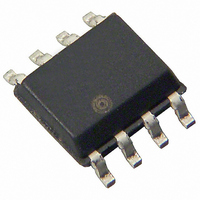
Manufacturer Part Number
EPCS1SI8N
Description
IC CONFIG DEVICE 1MBIT 8-SOIC
Manufacturer
Altera
Series
EPCSr
Datasheet
1.EPCS1SI8.pdf
(38 pages)
Specifications of EPCS1SI8N
Programmable Type
In System Programmable
Memory Size
1Mb
Voltage - Supply
3 V ~ 3.6 V
Operating Temperature
-40°C ~ 85°C
Package / Case
8-SOIC (0.154", 3.90mm Width)
Lead Free Status / RoHS Status
Lead free / RoHS Compliant
Other names
544-1242-5
Available stocks
Company
Part Number
Manufacturer
Quantity
Price
Company:

Part Number:
EPCS1SI8N
Manufacturer:
ALTERA
Quantity:
672
Part Number:
EPCS1SI8N
Manufacturer:
ALTERA/阿尔特拉
Quantity:
20 000


3–14
Operation Codes
Configuration Handbook (Complete Two-Volume Set)
Table 3–6. Address Range for Sectors in EPCS4 (Part 2 of 2)
Table 3–7. Address Range for Sectors in EPCS1
This section describes the operations that can be used to access the memory in serial
configuration devices. The DATA, DCLK, ASDI, and nCS signals access the memory in
serial configuration devices. All serial configuration device operation codes,
addresses and data are shifted in and out of the device serially, with the most
significant bit (MSB) first.
The device samples the active serial data input on the first rising edge of the DCLK
after the active low chip select (nCS) input signal is driven low. Shift the operation
code (MSB first) serially into the serial configuration device through the active serial
data input (ASDI) pin. Each operation code bit is latched into the serial configuration
device on the rising edge of the DCLK.
Different operations require a different sequence of inputs. While executing an
operation, you must shift in the desired operation code, followed by the address
bytes, data bytes, both, or neither. The device must drive nCS high after the last bit of
the operation sequence is shifted in.
operation supported by the serial configuration devices.
For the read byte, read status, and read silicon ID operations, the shifted-in operation
sequence is followed by data shifted out on the DATA pin. You can drive the nCS pin
high after any bit of the data-out sequence is shifted out.
For the write byte, erase bulk, erase sector, write enable, write disable, and write
status operations, drive the nCS pin high exactly at a byte boundary (drive the nCS
pin high a multiple of eight clock pulses after the nCS pin is driven low); otherwise,
the operation is rejected and is not executed.
All attempts to access the memory contents while a write or erase cycle is in progress
will not be granted, and the write or erase cycle will continue unaffected.
Chapter 3: Serial Configuration Devices (EPCS1, EPCS4, EPCS16, EPCS64, and EPCS128) Data Sheet
Sector
Sector
1
0
3
2
1
0
Table 3–8
H'10000
H'00000
H'18000
H'10000
H'08000
H'00000
Address Range (Byte Addresses in HEX)
Address Range (Byte Addresses in HEX)
Start
Start
lists the operation sequence for every
Serial Configuration Device Memory Access
© December 2009
H'1FFFF
H'0FFFF
H'1FFFF
H'17FFF
H'0FFFF
H'07FFF
End
End
Altera Corporation
Related parts for EPCS1SI8N
Image
Part Number
Description
Manufacturer
Datasheet
Request
R

Part Number:
Description:
(EPCS1 - EPCS64) Serial Configuration Devices
Manufacturer:
Altera Corporation
Datasheet:

Part Number:
Description:
IC CONFIG DEVICE 1MBIT 8-DIP
Manufacturer:
Altera
Datasheet:

Part Number:
Description:
IC CONFIG DEVICE 1.6MBIT 20-PLCC
Manufacturer:
Altera
Datasheet:
Part Number:
Description:
IC CONFIG DEVICE 1.6MBIT 20-PLCC
Manufacturer:
Altera
Datasheet:

Part Number:
Description:
IC CONFIG DEVICE 1.6MBIT 32-TQFP
Manufacturer:
Altera
Datasheet:
Part Number:
Description:
IC CONFIG DEVICE 1.6MBIT 32-TQFP
Manufacturer:
Altera
Datasheet:
Part Number:
Description:
IC CONFIG DEVICE 1.6MBIT 20-PLCC
Manufacturer:
Altera
Datasheet:
Part Number:
Description:
IC CONFIG DEVICE 1.6MBIT 20-PLCC
Manufacturer:
Altera
Datasheet:

Part Number:
Description:
IC CONFIG DEVICE 8MBIT 100-PQFP
Manufacturer:
Altera
Datasheet:
Part Number:
Description:
IC CONFIG DEVICE 1.6MBIT 32-TQFP
Manufacturer:
Altera
Datasheet:
Part Number:
Description:
IC CONFIG DEVICE 1.6MBIT 32-TQFP
Manufacturer:
Altera
Datasheet:
Part Number:
Description:
IC CONFIG DEVICE 16MBIT 100-PQFP
Manufacturer:
Altera
Datasheet:
Part Number:
Description:
IC CONFIG DEVICE 16MBIT 100-PQFP
Manufacturer:
Altera
Datasheet:
Part Number:
Description:
IC CONFIG DEVICE 16MBIT 100-PQFP
Manufacturer:
Altera
Datasheet: