EPCS1SI8N Altera, EPCS1SI8N Datasheet - Page 17
EPCS1SI8N
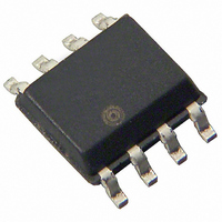
Manufacturer Part Number
EPCS1SI8N
Description
IC CONFIG DEVICE 1MBIT 8-SOIC
Manufacturer
Altera
Series
EPCSr
Datasheet
1.EPCS1SI8.pdf
(38 pages)
Specifications of EPCS1SI8N
Programmable Type
In System Programmable
Memory Size
1Mb
Voltage - Supply
3 V ~ 3.6 V
Operating Temperature
-40°C ~ 85°C
Package / Case
8-SOIC (0.154", 3.90mm Width)
Lead Free Status / RoHS Status
Lead free / RoHS Compliant
Other names
544-1242-5
Available stocks
Company
Part Number
Manufacturer
Quantity
Price
Company:

Part Number:
EPCS1SI8N
Manufacturer:
ALTERA
Quantity:
672
Part Number:
EPCS1SI8N
Manufacturer:
ALTERA/阿尔特拉
Quantity:
20 000


Chapter 3: Serial Configuration Devices (EPCS1, EPCS4, EPCS16, EPCS64, and EPCS128) Data Sheet
Serial Configuration Device Memory Access
Table 3–11. Block Protection Bits in EPCS16 (Part 1 of 2)
© December 2009
BP2
Bit
0
0
0
0
1
1
Status Register
Content
BP1
Bit
0
0
1
1
0
0
BP0
Altera Corporation
Bit
0
1
0
1
0
1
Resetting the write enable latch bit to 0 indicates that no write or erase cycle will be
accepted. Set the write enable latch bit to 1 before every write bytes, write status,
erase bulk, and erase sector operation.
The non-volatile block protect bits determine the area of the memory protected from
being written or erased unintentionally.
protected area in the serial configuration devices with reference to the block protect
bits. The erase bulk operation is only available when all the block protect bits are 0.
When any of the block protect bits are set to 1, the relevant area is protected from
being written by write bytes operations or erased by erase sector operations.
Table 3–9. Block Protection Bits in EPCS1
Table 3–10. Block Protection Bits in EPCS4
None
Upper 32nd (Sector 31)
Upper sixteenth (two sectors: 30 and 31)
Upper eighth (four sectors: 28 to 31)
Upper quarter (eight sectors: 24 to 31)
Upper half (sixteen sectors: 16 to 31)
BP2 Bit
BP1 Bit
Status Register Content
0
0
0
0
1
1
1
1
0
0
1
1
Status Register Content
BP1 Bit
Protected Area
0
0
1
1
0
0
1
1
BP0 Bit
0
1
0
1
BP0 Bit
0
1
0
1
0
1
0
1
None
Sector 3
Two sectors: 2 and 3
All sectors
Memory Content
None
Sector 7
Sectors 6 and 7
Four sectors: 4 to 7
All sectors
All sectors
All sectors
All sectors
Protected Area
Table 3–9
Protected Area
All sectors (32 sectors 0 to 31)
Lower 31/32nds (31 sectors: 0 to 30)
Lower 15/16ths (30 sectors: 0 to 29)
Lower seven-eighths (28 sectors: 0 to 27)
Lower three-quarters (24 sectors: 0 to 23)
Lower half (16 sectors: 0 to 15)
Configuration Handbook (Complete Two-Volume Set)
through
Memory Content
Memory Content
Unprotected Area
Table 3–13
All four sectors: 0 to 3
Three sectors: 0 to 2
Two sectors: 0 and 1
None
All eight sectors: 0 to 7
Seven sectors: 0 to 6
Six sectors: 0 to 5
Four sectors: 0 to 3
None
None
None
None
Unprotected Area
Unprotected Area
list the
3–17
Related parts for EPCS1SI8N
Image
Part Number
Description
Manufacturer
Datasheet
Request
R

Part Number:
Description:
(EPCS1 - EPCS64) Serial Configuration Devices
Manufacturer:
Altera Corporation
Datasheet:

Part Number:
Description:
IC CONFIG DEVICE 1MBIT 8-DIP
Manufacturer:
Altera
Datasheet:

Part Number:
Description:
IC CONFIG DEVICE 1.6MBIT 20-PLCC
Manufacturer:
Altera
Datasheet:
Part Number:
Description:
IC CONFIG DEVICE 1.6MBIT 20-PLCC
Manufacturer:
Altera
Datasheet:

Part Number:
Description:
IC CONFIG DEVICE 1.6MBIT 32-TQFP
Manufacturer:
Altera
Datasheet:
Part Number:
Description:
IC CONFIG DEVICE 1.6MBIT 32-TQFP
Manufacturer:
Altera
Datasheet:
Part Number:
Description:
IC CONFIG DEVICE 1.6MBIT 20-PLCC
Manufacturer:
Altera
Datasheet:
Part Number:
Description:
IC CONFIG DEVICE 1.6MBIT 20-PLCC
Manufacturer:
Altera
Datasheet:

Part Number:
Description:
IC CONFIG DEVICE 8MBIT 100-PQFP
Manufacturer:
Altera
Datasheet:
Part Number:
Description:
IC CONFIG DEVICE 1.6MBIT 32-TQFP
Manufacturer:
Altera
Datasheet:
Part Number:
Description:
IC CONFIG DEVICE 1.6MBIT 32-TQFP
Manufacturer:
Altera
Datasheet:
Part Number:
Description:
IC CONFIG DEVICE 16MBIT 100-PQFP
Manufacturer:
Altera
Datasheet:
Part Number:
Description:
IC CONFIG DEVICE 16MBIT 100-PQFP
Manufacturer:
Altera
Datasheet:
Part Number:
Description:
IC CONFIG DEVICE 16MBIT 100-PQFP
Manufacturer:
Altera
Datasheet: