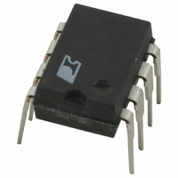
TNY256PN Power Integrations, TNY256PN Datasheet - Page 8

TNY256PN
Manufacturer Part Number
TNY256PN
Description
IC OFFLINE SWIT OTP UVLO HV 8DIP
Manufacturer
Power Integrations
Series
TinySwitch® Plusr
Datasheet
1.TNY256YN.pdf
(20 pages)
Specifications of TNY256PN
Output Isolation
Isolated
Frequency Range
115 ~ 140kHz
Voltage - Output
700V
Power (watts)
10W
Operating Temperature
-40°C ~ 150°C
Package / Case
8-DIP (0.300", 7.62mm)
Output Voltage
5.8 V
Input / Supply Voltage (max)
265 VAC
Input / Supply Voltage (min)
85 VAC
Duty Cycle (max)
69 %
Switching Frequency
130 KHz
Supply Current
255 uA
Operating Temperature Range
- 40 C to + 150 C
Mounting Style
Through Hole
Lead Free Status / RoHS Status
Lead free / RoHS Compliant
Other names
596-1171-5
TNY256PN
TNY256PN
Available stocks
Company
Part Number
Manufacturer
Quantity
Price
Company:
Part Number:
TNY256PN
Manufacturer:
POWER
Quantity:
3 000
Company:
Part Number:
TNY256PN
Manufacturer:
POWER
Quantity:
15 000
Part Number:
TNY256PN
Manufacturer:
POWER
Quantity:
20 000
Layout
Single Point Grounding
Use a single point ground connection at the SOURCE pin for the
BYPASS pin capacitor and the Input Filter Capacitor (see
Figure 13).
Primary Loop Area
The area of the primary loop that connects the input filter
capacitor, transformer primary and TinySwitch together, should
be kept as small as possible.
Primary Clamp Circuit
A clamp or snubber circuit is used to minimize peak voltage and
ringing on the DRAIN pin at turn-off. This can be achieved by
using an RC snubber for less than 3 W or an RCD clamp as
shown in Figure 13 for higher power. A Zener and diode clamp
across the primary or a single 550 V Zener clamp from DRAIN
to SOURCE can also be used. In all cases care should be taken
to minimize the circuit path from the snubber/clamp components
to the transformer and TinySwitch.
Thermal Considerations
Copper underneath the TinySwitch acts not only as a single point
ground, but also as a heatsink. The hatched area shown in
Figure13 should be maximized for good heat-sinking of
TinySwitch and output diode.
EN/UV pin layout optimization
The EN/UV pin connection to the opto-coupler should be kept
to an absolute minimum (less than 0.5 in.), and this connection
should be kept away from the DRAIN pin (minimum of 0.2 in.).
These distance limitations are critical only in applications
where an external under-voltage resistor (2 M ) is not used.
Figure 13. Recommended PC Layout for TinySwitch without Under-Voltage Lock Out Resistor.
8
TOP VIEW
HV
TNY256
+
–
C
7/01
Input Filter Capacitor
C
BP
BP
TinySwitch
S
S
Transformer
EN/UV
D
PRI
Safety Spacing
Capacitor
coupler
Opto-
Y1-
SEC
Y-Capacitor
The placement of the Y-capacitor should be directly from the
primary single point ground to the common/return terminal on
the secondary side. Such placement will maximize the EMI
benefit of the Y-capacitor.
Optocoupler
It is important to maintain the minimum circuit path from the
optocoupler transistor to the TinySwitch EN/UV and SOURCE
pins to minimize noise coupling.
Output Diode
For best performance, the area of the loop connecting the
secondary winding, the Output Diode and the Output Filter
Capacitor, should be minimized. See Figure13 for optimized
layout. In addition, sufficient copper area should be provided
at the anode and cathode terminals of the diode to adequately
heatsink the diode under output short circuit conditions.
Input and Output Filter Capacitors
There are constrictions in the traces connected to the input and
output filter capacitors. These constrictions are present for two
reasons. The first is to force all the high frequency currents to
flow through the capacitor (if the trace were wide then it could
flow around the capacitor). Secondly, the constrictions minimize
the heat transferred from the TinySwitch to the input filter
capacitor and from the secondary diode to the output filter
capacitor. The common/return (the negative output terminal in
Figure13) terminal of the output filter capacitor should be
connected with a short, low resistance path to the secondary
winding. In addition, the common/return output connection
should be taken directly from the secondary winding pin and not
from the Y-capacitor connection point.
Output Filter Capacitor
–
Out
DC
+
Maximize hatched copper
areas (
heat sinking
) for optimum
PI-2360-012199


