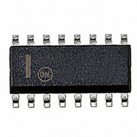
MC33364D ON Semiconductor, MC33364D Datasheet - Page 4

MC33364D
Manufacturer Part Number
MC33364D
Description
IC CTRLR SMPS OTP UVLO 16SOIC
Manufacturer
ON Semiconductor
Series
GreenLine™r
Datasheet
1.MC33364DR2G.pdf
(16 pages)
Specifications of MC33364D
Output Isolation
Isolated
Frequency Range
104 ~ 800kHz
Voltage - Input
7.6 ~ 16 V
Voltage - Output
700V
Power (watts)
550mW
Operating Temperature
-25°C ~ 150°C
Package / Case
16-SOIC (0.154", 3.90mm Width) 14 leads
Number Of Outputs
1
Output Voltage
4.90 V to 5.20 V
Output Current
600 mA
Mounting Style
SMD/SMT
Operating Supply Voltage
16 V
Maximum Operating Temperature
+ 125 C
Fall Time
28 ns
Minimum Operating Temperature
- 25 C
Rise Time
67 ns
Synchronous Pin
No
Topology
Flyback
Lead Free Status / RoHS Status
Contains lead / RoHS non-compliant
Other names
MC33364DOS
Available stocks
Company
Part Number
Manufacturer
Quantity
Price
Part Number:
MC33364D
Manufacturer:
FREESCALE
Quantity:
20 000
Part Number:
MC33364D1G
Manufacturer:
ON/安森美
Quantity:
20 000
Part Number:
MC33364D1R2G
Manufacturer:
ON/安森美
Quantity:
20 000
Part Number:
MC33364D2G
Manufacturer:
ON/安森美
Quantity:
20 000
Company:
Part Number:
MC33364D2R2
Manufacturer:
PULSE
Quantity:
2 400
Part Number:
MC33364D2R2G
Manufacturer:
ON/安森美
Quantity:
20 000
NOTE:
Stresses exceeding Maximum Ratings may damage the device. Maximum Ratings are stress ratings only. Functional operation above the
Recommended Operating Conditions is not implied. Extended exposure to stresses above the Recommended Operating Conditions may affect
device reliability.
NOTE:
PIN DESCRIPTION
MAXIMUM RATINGS
Power Supply Voltage (Operating)
Line Voltage
Current Sense, Compensation,
Zero Current Detect Input
Restart Diode Current
Power Dissipation and Thermal Characteristics
Operating Junction Temperature
Operating Ambient Temperature
Storage Temperature Range
Voltage Feedback, Restart Delay and Zero Current Input Voltage
8 (NA)
10 (5)
11 (6)
12 (7)
16 (8)
1 (1)
3 (2)
4 (3)
6 (4)
9 (5)
D1 and D2 Suffix, Plastic Package Case 751
D Suffix, Plastic Package Case 751B--05
Pin
Maximum Power Dissipation @ T
Thermal Resistance, Junction--to--Air
Maximum Power Dissipation @ T
Thermal Resistance, Junction--to--Air
For further information please refer to the following Application Notes;
AN1594: Critical Conduction Mode, Flyback Switching Power Supply Using the MC33364.
AN1681: How to keep a Flyback Switch--Mode Power Supply Stable with a Critical--Mode Controller.
ESD data available upon request.
Zero Current Detect
Voltage Feedback
Frequency Clamp
Current Sense
Gate Drive
Function
A GND
P GND
Line
V
V
CC
ref
(T
A
= 25C, unless otherwise noted.)
Rating
A
A
The ZCD Pin ensures critical conduction mode. ZCD monitors the voltage on the auxiliary winding,
during the demagnetization phase of the transformer, comparing it to an internal reference. The
ZCD sets the latch for the output driver.
The Current Sense Pin monitors the current in the power switch by measuring the voltage across
a resistor. Leading Edge Blanking is utilized to prevent false triggering. The voltage is compared to
a resistor divider connected to the Voltage Feedback Pin. A 110 mV voltage off--set is applied to
compensate the natural optocoupler saturation voltage.
The Voltage Feedback Pin is typically connected to the collector of the optocoupler for feedback
from the isolated secondary output. The Feedback is connected to the V
providing bias for the external optocoupler.
The V
The Frequency Clamp Pin ensures a minimum off--time value, typically 6.9 ms. It prevents the
MOSFET from restarting within a fixed (33364D1) or adjustable (33364D) delay. The minimum
off--time is disabled in the 33364D2. Therefore the maximum switching frequency cannot exceed
1/(T
This pin is the ground for the internal circuitry excluding the gate drive stage.
This pin is the ground for the gate drive stage.
The gate drive is the output to drive the gate of the power MOSFET.
Provides the voltage for all internal circuitry including the gate drive stage and V
Undervoltage Lockout with hysteresis.
The Line Pin provides the initial power to the V
current source, eliminating the need for an external startup network.
= 70C
= 70C
ON
ref
+ T
Pin is a buffered internal 5.0 V reference with Undervoltage Lockout.
OFFmin
).
http://onsemi.com
4
Description
CC
Symbol
V
R
R
V
V
T
P
P
pins. Internally the line pin is a high voltage
T
T
Line
I
I
θJA
θJA
stg
CC
in1
in
in
A
D
D
J
--25 to +125
--55 to +150
--1.0 to +10
ref
Value
5.0
700
450
178
550
145
150
5.0
16
Pin via a 5 k resistor
ref
. This pin has
C/W
C/W
Unit
mW
mW
mA
mA
C
C
C
V
V
V


