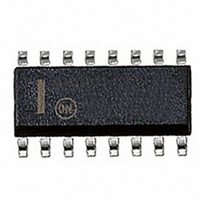
MC33364D ON Semiconductor, MC33364D Datasheet - Page 8

MC33364D
Manufacturer Part Number
MC33364D
Description
IC CTRLR SMPS OTP UVLO 16SOIC
Manufacturer
ON Semiconductor
Series
GreenLine™r
Datasheet
1.MC33364DR2G.pdf
(16 pages)
Specifications of MC33364D
Output Isolation
Isolated
Frequency Range
104 ~ 800kHz
Voltage - Input
7.6 ~ 16 V
Voltage - Output
700V
Power (watts)
550mW
Operating Temperature
-25°C ~ 150°C
Package / Case
16-SOIC (0.154", 3.90mm Width) 14 leads
Number Of Outputs
1
Output Voltage
4.90 V to 5.20 V
Output Current
600 mA
Mounting Style
SMD/SMT
Operating Supply Voltage
16 V
Maximum Operating Temperature
+ 125 C
Fall Time
28 ns
Minimum Operating Temperature
- 25 C
Rise Time
67 ns
Synchronous Pin
No
Topology
Flyback
Lead Free Status / RoHS Status
Contains lead / RoHS non-compliant
Other names
MC33364DOS
Available stocks
Company
Part Number
Manufacturer
Quantity
Price
Part Number:
MC33364D
Manufacturer:
FREESCALE
Quantity:
20 000
Part Number:
MC33364D1G
Manufacturer:
ON/安森美
Quantity:
20 000
Part Number:
MC33364D1R2G
Manufacturer:
ON/安森美
Quantity:
20 000
Part Number:
MC33364D2G
Manufacturer:
ON/安森美
Quantity:
20 000
Company:
Part Number:
MC33364D2R2
Manufacturer:
PULSE
Quantity:
2 400
Part Number:
MC33364D2R2G
Manufacturer:
ON/安森美
Quantity:
20 000
Current Sense and Feedback Regulation
Sense (CS) pin and Feedback (FB) pin. The FB pin is
internally pulled up with a 5 kOhm resistor from the 5 V
V
this functional block. The following equation describes the
relation between the voltages of the FB and CS pins, V
and V
signal from the opto coupler and the FB pin is opened. It
gives V
1.15 V. When the voltage exceeds 1.15 V, the current sense
comparator turns on and terminates the MOSFET
conduction. It stops current flowing through the sense
resistor (R
maximum MOSFET drain current by the following
equation.
pulled down by the opto coupler current and the duty ratio
is reduced. The output voltage is then regulated.
250 ns propagation delay to prevent false triggering due to
parasitics in the CS pin. It makes a minimum on- -time of the
MOSFET (t
Thermal Shutdown
condition and protect the device from overheating. When
temperature is over 180_C, the Drive output and startup
circuit block are disable. The device resumes operation
when temperature falls below 130_C.
Gate Drive Output
designed for direct drive of power MOSFET. The Drive
Output typical rise and fall times are 50 ns with a 1.0 nF
load. Unbalanced Source and Sink eliminates the need for an
external resistor between the device Drive output and the
Gate of the external MOSFET. Additional internal circuitry
has been added to keep the Drive Output in a sinking mode
whenever the UVLO is active. This characteristic eliminates
the need for an external gate pull- -down resistor.
ref
Current- -mode control is implemented with the Current
When the output is short circuited, there is no feedback
When the output voltage is too high, the FB pin voltage is
There is a Leading Edge Blanking (LEB) circuit with
There is a thermal shutdown block to prevent overheating
The IC contains a CMOS output driver specifically
. There is a resistor divider circuit and a 0.1 V offset in
CS
FB
Maximum Drain Current = 1.15∕R sense
respectively.
= 5 V and the maximum voltage of the CS pin is
Sense
on(min)
V CS(max) = V FB ∕4 − 0.1 V
) and hence the sense resistor limits the
).
http://onsemi.com
FB
8
Frequency Clamp Options
switching frequency. The switching frequency can increase
dramatically to hundreds of kHz when the output current is
too low or vanishes. It is a big problem when EMI above
150 kHz is concerned. Frequency Clamp (FC) is an optional
feature in the device to limit the upper switching frequency
to nominal 126 kHz by inserting a minimum off- -time
(t
maximum frequency (f
maximum frequency is reached. The minimum off- -time is
immediately counted after the driving signal goes low. If the
ZCD signal comes within this minimum off- -time, the ZCD
information is ignored until the minimum off- -time expires.
The next ZCD signal starts the MOSFET conduction.
adjustable minimum off- -time by external resistor,
MC33364D1 - - 6.9 us fixed minimum off- -time, and
MC33364D2 - - no minimum off- -time (FC disable).
minimum off- -time (or the maximum frequency) externally
in Figure 11. If the FC pin is opened, the minimum off- -time
is fixed at 6.9 us. If the FC pin is grounded, the clamp is
disabled, and the SMPS will always operate in critical mode.
It is generally not recommended to sink or source more than
80 uA from the FC pin because high currents may cause
unstable operation.
off(min)
The drawback of critical conduction mode is variable
The SMPS is forced to operate in DCM when the
There are three available FC options: MC33364D - -
The MC33364D has a FC pin, which can vary the
). When a minimum off- -time is inserted, the
Figure 11. Frequency Clamp Setting
toff = 6.9us
Increase toff
FC
FC
Vref
f max =
max
t on(min) + t off(min)
) limit is set.
(FC disable)
toff = 0us
GND
1
FC
Decrease toff
FC
GND


