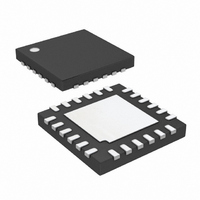
LTC4007EUFD-1#TRPBF Linear Technology, LTC4007EUFD-1#TRPBF Datasheet - Page 7

LTC4007EUFD-1#TRPBF
Manufacturer Part Number
LTC4007EUFD-1#TRPBF
Description
IC CHARGER BATTERY 4A 24-QFN
Manufacturer
Linear Technology
Type
Battery Chargerr
Datasheet
1.LTC4007EUFD-1PBF.pdf
(24 pages)
Specifications of LTC4007EUFD-1#TRPBF
Function
Charge Management
Battery Type
Lithium-Ion (Li-Ion)
Voltage - Supply
6 V ~ 28 V
Operating Temperature
-40°C ~ 85°C
Mounting Type
Surface Mount
Package / Case
24-WFQFN Exposed Pad
Output Current
4A
Output Voltage
4.1/4.2V
Operating Supply Voltage (min)
6V
Operating Supply Voltage (max)
28V
Operating Temp Range
-40C to 85C
Package Type
QFN
Mounting
Surface Mount
Pin Count
24
Operating Temperature Classification
Industrial
Lead Free Status / RoHS Status
Lead free / RoHS Compliant
Available stocks
Company
Part Number
Manufacturer
Quantity
Price
PI FU CTIO S
PROG (Pin 9): Current Programming/Monitoring Input/
Output. An external resistor to GND programs the peak
charging current in conjunction with the current sensing
resistor. The voltage at this pin provides a linear indication
of charging current. Peak current is equivalent to 1.19V.
Zero current is approximately 0.3V. A capacitor from
PROG to ground is required to filter higher frequency
components. The maximum resistance to ground is 100k.
Values higher than 100k can cause the charger to shut
down.
I
digital output. Internal 10µA pull-up to 3.5V. Pulled low if
the charger current is being reduced by the input current
limiting function. The pin is capable of sinking at least
100µA. If V
pull-up.
CSP (Pin 11): Current Amplifier CA1 Input. The CSP and
BAT pins measure the voltage across the sense resistor,
R
quired for both peak and average current mode operation.
BAT (Pin 12): Battery Sense Input and the Negative
Reference for the Current Sense Resistor. A precision
internal resistor divider sets the final float potential on this
pin. The resistor divider is disconnected during shutdown.
CHEM (Pin 13):Select 4.1V or 4.2V cell chemistry by
connecting the pin to GND or open, respectively. Internal
14µA pull-up to 5.3V. Can also be driven with open-
collector/drain logic levels.
FLAG (Pin 14): Active low open-drain output that indi-
cates when charging current has declined to 10% of
maximum programmed current. A pull-up resistor is
required if this function is used. The pin is capable of
sinking at least 100µA.
CL
SENSE
U
(Pin 10): Input Current Limit Indicator. Active low
, to provide the instantaneous current signals re-
U
LOGIC
is greater than 3.3V, add an external
U
CLP (Pin 15): Positive input to the supply current limiting
amplifier, CL1. The threshold is set at 100mV above the
voltage at the CLN pin. When used to limit supply current,
a filter is needed to filter out the switching noise. If no
current limit function is desired, connect this pin to CLN.
CLN (Pin 16): Negative Reference for the Input Current
Limit Amplifier, CL1. This pin also serves as the power
supply for the IC. A 10µF to 22µF bypass capacitor should
be connected as close as possible to this pin.
TGATE (Pin 17): Drives the top external P-channel MOSFET
of the battery charger buck converter.
PGND (Pin 18): High Current Ground Return for the BGATE
Driver.
NC (Pin 19): No Connect.
BGATE (Pin 20): Drives the bottom external N-channel
MOSFET of the battery charger buck converter.
INFET (Pin 21): Drives the Gate of the External Input PFET.
SHDN (Pin 22): Charger is shut down and timer is reset
when this pin is HIGH. Internal 10µA pull-up to 3.5V. This
pin can also be used to reset the charger by applying a
positive pulse that is a minimum of 0.1µs long.
DCIN (Pin 23): External DC Power Source Input. Bypass
this pin with at least 0.01µF. See Applications Information.
CHG (Pin 24): Charge Status Output. When the battery is
being charged, the CHG pin is pulled low by an internal
N-channel MOSFET. Internal 10µA pull-up to 3.5V. If
V
timer function can be defeated by forcing this pin below 1V
(or connecting it to GND).
Exposed Pad (Pin 25): The exposed pad, GND and PGND
should be connected together with a low ohmic connec-
tion.
LOGIC
is greater than 3.3V, add an external pull-up. The
LTC4007-1
40071f
7


