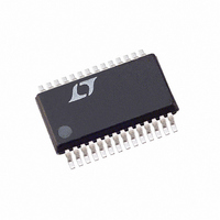
LT1505CG Linear Technology, LT1505CG Datasheet - Page 10

LT1505CG
Manufacturer Part Number
LT1505CG
Description
IC BATT CHARGER CONST I/V 28SSOP
Manufacturer
Linear Technology
Datasheet
1.LT1505CG-1PBF.pdf
(16 pages)
Specifications of LT1505CG
Function
Charge Management
Battery Type
Li-Ion, NiCd, NiMH
Voltage - Supply
11 V ~ 24 V
Operating Temperature
0°C ~ 70°C
Mounting Type
Surface Mount
Package / Case
28-SSOP (0.200", 5.30mm Width)
Lead Free Status / RoHS Status
Contains lead / RoHS non-compliant
Available stocks
Company
Part Number
Manufacturer
Quantity
Price
Company:
Part Number:
LT1505CG
Manufacturer:
LT
Quantity:
5 510
Part Number:
LT1505CG
Manufacturer:
LT/凌特
Quantity:
20 000
Part Number:
LT1505CG#PBF
Manufacturer:
LINEAR/凌特
Quantity:
20 000
Part Number:
LT1505CG-1
Manufacturer:
LT
Quantity:
20 000
Part Number:
LT1505CG-1#TRPBF
Manufacturer:
LINEAR/凌特
Quantity:
20 000
OPERATION
APPLICATIONS
Input and Output Capacitors
In the 4A Lithium Battery Charger (Figure 1), the input
capacitor (C
ripple current in the converter, so it must have adequate
ripple current rating. Worst-case RMS ripple current will
be equal to one half of output charging current. Actual
capacitance value is not critical. Solid tantalum capacitors
such as the AVX TPS and Sprague 593D series have high
ripple current rating in a relatively small surface mount
package, but caution must be used when tantalum capaci-
tors are used for input bypass . High input surge currents
can be created when the adapter is hot-plugged to the
charger and solid tantalum capacitors have a known
failure mechanism when subjected to very high turn-on
surge currents. Highest possible voltage rating on the
LT1505
The LT1505 is a synchronous current mode PWM step-
down (buck) switcher. The battery DC charge current is pro-
grammed by a resistor R
the PROG pin and the ratio of sense resistors R
(see Block Diagram). Amplifier CA1 converts the charge cur-
rent through R
I
pares the output of CA1 with the programmed current and
drives the PWM loop to force them to be equal. High DC
accuracy is achieved with averaging capacitor C
that I
through R1 and generates a ramp signal that is fed to the
PWM control comparator C1 through buffer B1 and level
shift resistors R2 and R3, forming the current mode inner
loop. The BOOST pin supplies the topside power switch gate
drive. The LT1505 generates an 9.1V V
and V
CA1 with a voltage higher than V
cation. For batteries like lithium that require both constant-
current and constant-voltage charging, the 0.5% 2.465V
reference and the amplifier VA reduce the charge current
when battery voltage reaches the preset level. For NiMH and
NiCd, VA can be used for overvoltage protection.
The amplifier CL1 monitors and limits the input current,
normally from the AC adapter, to a preset level (92mV/R
10
BAT
• RS1/RS2) fed into the PROG pin. Amplifier CA2 com-
PROG
BOOSTC
has both AC and DC components. I
IN
. BOOSTC pin supplies the current amplifier
) is assumed to absorb all input switching
S1
U
to a much lower current I
U
PROG
INFORMATION
U
(or a DAC output current) at
CC
for low dropout appli-
W
GBIAS
to power drives
PROG
S2
PROG
PROG
U
over R
(I
PROG
. Note
goes
S
S1
).
=
At input current limit, CL1 will supply the programming
current I
To prevent current shoot-through between topside and
lowside switches, comparators A3 and A4 assure that one
switch turns off before the other is allowed to turn on.
Comparator A12 monitors charge current level and turns
lowside switch off if it drops below 20% of the programmed
value (20mV across R
ous mode operation. Therefore sometimes even in con-
tinuous mode operation with light current level the lowside
switch stays off.
Comparator E6 monitors the charge current and signals
through the FLAG pin when the charger is in voltage mode
and the charge current level is reduced to 20%. This charge
complete signal can be used to start a timer for charge
termination.
The INFET pin drives an external P-channel FET for low
dropout application.
When input voltage is removed, V
body diode of the topside MOSFET. The LT1505 goes into
a low current, 10 A typical, sleep mode as V
below the battery voltage. To shut down the charger
simply pull the V
capacitor will minimize problems. Consult the manufac-
turer before use. Alternatives include new high capacity
ceramic (at least 20 F) from Tokin or United Chemi-Con/
Marcon, et al.
The output capacitor (C
output switching current ripple. The general formula for
capacitor current is:
For example, V
and f = 200kHz, I
I
RMS
PROG
=
0.29 (V
, thus reducing battery charging current.
CC
C
(L1)(f)
RMS
pin or SHDN pin low with a transistor.
BAT
= 19V, V
S1
= 0.4A.
) 1 –
) to allow for inductor discontinu-
OUT
) is also assumed to absorb
V
V
BAT
BAT
CC
CC
= 12.6V, L1 = 15 H,
will be held up by the
CC
drops
1505fc


