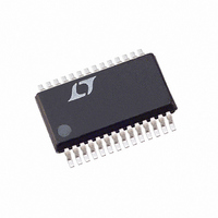
LT1505CG Linear Technology, LT1505CG Datasheet - Page 6

LT1505CG
Manufacturer Part Number
LT1505CG
Description
IC BATT CHARGER CONST I/V 28SSOP
Manufacturer
Linear Technology
Datasheet
1.LT1505CG-1PBF.pdf
(16 pages)
Specifications of LT1505CG
Function
Charge Management
Battery Type
Li-Ion, NiCd, NiMH
Voltage - Supply
11 V ~ 24 V
Operating Temperature
0°C ~ 70°C
Mounting Type
Surface Mount
Package / Case
28-SSOP (0.200", 5.30mm Width)
Lead Free Status / RoHS Status
Contains lead / RoHS non-compliant
Available stocks
Company
Part Number
Manufacturer
Quantity
Price
Company:
Part Number:
LT1505CG
Manufacturer:
LT
Quantity:
5 510
Part Number:
LT1505CG
Manufacturer:
LT/凌特
Quantity:
20 000
Part Number:
LT1505CG#PBF
Manufacturer:
LINEAR/凌特
Quantity:
20 000
Part Number:
LT1505CG-1
Manufacturer:
LT
Quantity:
20 000
Part Number:
LT1505CG-1#TRPBF
Manufacturer:
LINEAR/凌特
Quantity:
20 000
PIN
LT1505
BOOST (Pin 1): This pin is used to bootstrap and supply
power for the topside power switch gate drive and control
circuity. In normal operation, V
internally generated 8.6V regulator V
+ 9.1V when TGATE is high. Do not force an external
voltage on BOOST pin.
TGATE (Pin 2): This pin provides gate drive to the topside
power FET. When TGATE is driven on, the gate voltage will
be approximately equal to V
5 to 10 should be used from this pin to the gate of the
topside FET.
SW (Pin 3): This pin is the reference point for the floating
topside gate drive circuitry. It is the common connection
for the top and bottom side switches and the output
inductor. This pin switches between ground and V
very high dv/dt rates. Care needs to be taken in the PC
layout to keep this node from coupling to other sensitive
nodes. A 1A Schottky clamp diode should be placed from
this pin to the ground pin, using very short traces to
prevent the chip substrate diode from turning on. See
Applications Information for more details.
SYNC (Pin 4): Synchronization Input. The LT1505 can be
synchronized to an external clock with pulses that have
duty cycles between 10% and 95%. An internal one shot
that is triggered on the rising edge of the sync pulse makes
this input insensitive to the duty cycle of the sync pulse.
The input voltage range on this pin is 0V to 20V. This pin
can float if not used.
SHDN (Pin 5): Shutdown. When this pin is pulled below 1V,
switching will stop, GBIAS will go low and the input cur-
rents of CA1 will be off. Note that input current of about 4 A
keeps the device in shutdown unless an external pull-up
signal is applied. The voltage range on this pin is 0V to V
AGND (Pin 6): Low Current Analog Ground.
UV (Pin 7): Undervoltage Lockout Input. The rising thresh-
old is 6.7V with a hysteresis of 0.5V. Switching stops in
undervoltage lockout. When the input supply (normally
the wall adapter output) to the chip is removed, the UV pin
must be pulled down to below 0.7V (a 5k resistor from
adapter output to GND is required), otherwise the reverse-
battery current will be approximately 200 A instead of
10 A. Do not leave the UV pin floating. If it is connected
6
U
FUNCTIONS
U
U
SW
+ 6.6V. A series resistor of
BOOST
GBIAS
is powered from an
, V
BOOST
CC
with
V
CC
CC
.
to V
lockout will be effective. Maximum voltage allowed on this
pin is V
INFET (Pin 8): For very low dropout applications, an
external P-channel MOSFET can be used to connect the
input supply to V
PFET. The gate drive is clamped to 8V below V
is driven on (low) when V
V
The body diode of the PFET is used to pull up V
on the LT1505.
CLP (Pin 9): LT1505: Positive Input to the Input Current
Limit Amplifier CL1. The threshold is set at 92mV. When
used to limit input current, a filter is needed to filter out the
200kHz switching noise. (LT1505-1: No Connection.)
CLN (Pin 10): LT1505: Negative Input to the Input Current
Limit Amplifier CL1. When used, both CLP and CLN should
be connected to a voltage higher than 6V and normally
V
voltage allowed on both CLP and CLN is V
(LT1505-1: No Connection.)
COMP1 (Pin 11): LT1505: Compensation Node for the
Input Current Limit Amplifier CL1. At input adapter current
limit, this pin rises to 1V. By forcing COMP1 low with an
external transistor, amplifier CL1 will be disabled (no
adapter current limit). Output current is less than 0.2mA.
See the Figure 1 circuit for the required resistor and
capacitor values. (LT1505-1: connect to GND.)
CAP (Pin 12): A 0.1 F capacitor from CAP to ground is
needed to filter the sampled charging current signal. This
filtered signal is used to set the FLAG pin when the
charging current drops below 20% of the programmed
maximum charging current.
FLAG (Pin 13): This pin is an open-collector output that is
used to indicate the end of charge. The FLAG pin is driven
low when the charge current drops below 20% of the
programmed charge current. A pull-up resistor is
required if this function is used. This pin is capable of
sinking at least 1mA. Maximum voltage on this pin is V
4.1V (Pin 14), 4.2V (Pin 15), 3CELL (Pin 16), V
17): These four pins are used to select the battery voltage
using the preset internal resistor network. The V
UV
CC
IN
> 6.7V. The gate is off (high) when V
(to the V
with no resistor divider, the built-in 6.7V undervoltage
CC
.
CC
bypass capacitor for less noise). Maximum
CC
. This pin provides the gate drive for the
CC
> (V
BAT
CC
< (V
+ 0.2V) and
CC
BAT
CC
. The gate
CC
FB
+ 0.2V).
FB
to turn
+ 1V.
pin is
(Pin
1505fc
CC
.


