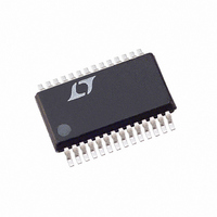
LT1505CG Linear Technology, LT1505CG Datasheet - Page 7

LT1505CG
Manufacturer Part Number
LT1505CG
Description
IC BATT CHARGER CONST I/V 28SSOP
Manufacturer
Linear Technology
Datasheet
1.LT1505CG-1PBF.pdf
(16 pages)
Specifications of LT1505CG
Function
Charge Management
Battery Type
Li-Ion, NiCd, NiMH
Voltage - Supply
11 V ~ 24 V
Operating Temperature
0°C ~ 70°C
Mounting Type
Surface Mount
Package / Case
28-SSOP (0.200", 5.30mm Width)
Lead Free Status / RoHS Status
Contains lead / RoHS non-compliant
Available stocks
Company
Part Number
Manufacturer
Quantity
Price
Company:
Part Number:
LT1505CG
Manufacturer:
LT
Quantity:
5 510
Part Number:
LT1505CG
Manufacturer:
LT/凌特
Quantity:
20 000
Part Number:
LT1505CG#PBF
Manufacturer:
LINEAR/凌特
Quantity:
20 000
Part Number:
LT1505CG-1
Manufacturer:
LT
Quantity:
20 000
Part Number:
LT1505CG-1#TRPBF
Manufacturer:
LINEAR/凌特
Quantity:
20 000
PIN
the noninverting input to the amplifier, VA in the Block
Diagram, that controls the charging current when the
device operates in constant voltage mode. The amplifier
VA controls the charging current to maintain the voltage
on the V
current for VA is approximately 3nA. The LT1505 incorpo-
rates a resistor divider that can be used to select the
correct voltage for either three or four 4.1V or 4.2V
lithium-ion cells. For three cells the 3CELL pin is shorted
to the V
nected. For 4.1V cells the 4.1V pin is connected to the V
pin and the 4.2V pin is not connected. For 4.2V cells the
4.2V pin is connected to V
connected. See the table below.
PRESET BATTERY VOLTAGE
12.3V (3 4.1V Cell)
16.4V (4 4.1V Cell)
12.6V (3 4.2V Cell)
16.8V (4 4.2V Cell)
For battery voltages other than the preset values, an
external resistor divider can be used. If an external divider
is used then the 4.1V, 4.2V and 3CELL pins should not be
connected and BAT2 pin should be grounded. To maintain
the tight voltage tolerance, the external resistors should
have better than 0.25% tolerance. Note that the V
float high and inhibit switching if it is left open.
V
the current mode PWM. Switching starts at 0.9V, higher
V
operation and reaches 1.1V at full charging current. A
capacitor of at least 0.33 F to GND filters out noise and
controls the rate of soft start. Pulling this pin low will stop
switching. Typical output current is 60 A.
PROG (Pin 19): This pin is for programming the charge
current and for system loop compensation. During normal
operation, V
more than 1mA is drawn out of the pin, switching will stop.
When a microprocessor controlled DAC is used to pro-
gram charging current, it must be capable of sinking
current at a compliance up to 2.465V.
C
C
U
(Pin 18): This is the control signal of the inner loop of
corresponds to higher charging current in normal
FUNCTIONS
FB
FB
pin at the reference voltage (2.465V). Input bias
U
pin. For four cells the 3CELL pin is not con-
PROG
stays at 2.465V. If it is shorted to GND or
U
PIN SELECTION
4.1V, V
4.1V, V
4.2V, V
4.2V, V
FB
FB
FB
FB
FB
and the 4.1V pin is not
, 3CELL Short Together
, Short Together, 3CELL Floats
, 3CELL Short Together
, Short Together, 3CELL Floats
FB
pin will
FB
BAT2 (Pin 20): This pin is used to connect the battery to
the internal preset voltage setting resistor. An internal
switch disconnects the internal divider from the battery
when the device is in shutdown or when power is discon-
nected. This disconnect function eliminates the current
drain due to the resistor divider. This pin should be
connected to the positive node of the battery if the internal
preset divider is used. This pin should be grounded if an
external divider is used. Maximum input voltage on this
pin is 20V.
SENSE (Pin 21): This pin is the noninverting input to the
current amplifier CA1 in the Block Diagram. Typical bias
current is – 50 A.
SPIN (Pin 22): This pin is for the internal amplifier CA1
bias. It must be connected as shown in the application
circuit.
BAT (Pin 23): Current Amplifier CA1 Inverting Input.
Typical bias current is – 50 A.
V
capacitor of 10 F or higher is required. Keep the lead
length to a minimum. V
Do not force V
battery present.
BOOSTC (Pin 25): This pin is used to bootstrap and supply
the current sense amplifier CA1 for very low dropout
condition. V
voltage. A diode and a capacitor are needed to get the
voltage from V
is always 3V or higher than V
floating or tied to V
lower than V
GBIAS (Pin 26): This is the output of the internal 9.1V
regulator to power the drivers and control circuits. This pin
must be bypassed to a ground plane with a minimum of
2.2 F ceramic capacitor. Switching will stop when V
drops below 7V.
BGATE (Pin 27): Low Side Power MOSFET Drive.
PGND (Pin 28): MOSFET Driver Power Ground. A solid
system ground plane is very important. See the LT1505
Demo Manual for further information.
CC
(Pin 24): Input Supply. For good bypass, a low ESR
CC
CC
BOOST
can be as low as only 0.4V above the battery
. Typical input current is 1mA.
CC
below V
CC
. If low dropout is not needed and V
. Do not force this pin to a voltage
CC
should be between 11V and 24V.
BAT
by more than 1V with the
BAT
, this pin can be left
LT1505
GBIAS
1505fc
7
CC


