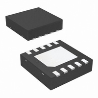
LM3658SDX/NOPB National Semiconductor, LM3658SDX/NOPB Datasheet - Page 10

LM3658SDX/NOPB
Manufacturer Part Number
LM3658SDX/NOPB
Description
IC USB/AC LI-ION CHARGER 10-LLP
Manufacturer
National Semiconductor
Type
Battery Chargerr
Datasheet
1.LM3658SD-ANOPB.pdf
(14 pages)
Specifications of LM3658SDX/NOPB
Function
Charge Management
Battery Type
Lithium-Ion (Li-Ion), Lithium-Polymer (Li-Pol)
Voltage - Supply
4.35 V ~ 6 V
Operating Temperature
-40°C ~ 85°C
Mounting Type
Surface Mount
Package / Case
10-WFDFN Exposed Pad
Output Current
25mA
Output Voltage
4.2V
Operating Supply Voltage (min)
4.35V
Operating Supply Voltage (max)
6V
Operating Temp Range
-40C to 85C
Package Type
LLP EP
Mounting
Surface Mount
Pin Count
10
Operating Temperature Classification
Industrial
For Use With
LM3658SDEV - BOARD EVALUATION LM3658SD
Lead Free Status / RoHS Status
Lead free / RoHS Compliant
Other names
LM3658SDX
Available stocks
Company
Part Number
Manufacturer
Quantity
Price
Company:
Part Number:
LM3658SDX/NOPB
Manufacturer:
TI
Quantity:
9 820
Part Number:
LM3658SDX/NOPB
Manufacturer:
TI/德州仪器
Quantity:
20 000
www.national.com
LDO MODE (AVAILABLE ONLY IN LM3658SD-B
VERSION)
The LM3658SD-B version enters LDO mode when the T
is floating and AC wall adapter is still connected to CHG_IN
pin. In LDO mode, STAT1 and STAT2 are both on. The
LM3658SD-B becomes a linear regulator capable of deliver-
ing 1A of source current. Normally the T
the thermistor from the battery pack for temperature monitor-
ing purpose. If this pin is disconnected, the LM3658SD-B
assumes that there is no battery present and will automati-
cally invoke the LDO mode. LDO mode allows applications to
operate without a battery provided that the AC wall adapter
supplies power to the CHG_IN pin. The LDO mode is not
possible in USB mode.
For the other versions of the LM3658, floating the T
not invoke LDO mode. Instead, it will go to suspend mode.
Please refer to “ Battery Temperature Monitoring” section for
more detail.
5 HOUR/ 10 HOUR SELECTABLE TIMER (AVAILABLE
ONLY IN LM3658SD-A VERSION)
The LM3658SD-A allows the user to select between 5 hour
or 10 hour timer based on the polarity of the USB_sel pin, in
both CHG_IN mode and USBpwr mode. By pulling the
USB_sel pin high, the timer is set to 5 hours. In the USBpwr
mode, the polarity of the USB_sel pin determines the charge
current as well as the timer. In CHG_IN mode, the polarity of
the USB_sel pin determines only the timer. The charge cur-
rent is set by the resistor at I
INPUT/OUTPUT BYPASS CAPACITORS
Care should be taken to support the stability of the charge
system by connecting a 1 µF capacitor as close as possible
to the BATT pin. An input capacitor ranging from 1.0 µF–
10.0 µF must be connected to the CHG_IN and USBpwr input
pins. Low cost ceramic capacitors can be selected.
set
pin.
s
pin is connected to
s
pin does
s
pin
10
THERMAL PERFORMANCE OF THE LLP PACKAGE
The LM3658 is a monolithic device with integrated power
FETs. For that reason, it is important to pay special attention
to the thermal impedance of the LLP package and to the PCB
layout rules in order to maximize power dissipation of the LLP
package.
The LLP package is designed for enhanced thermal perfor-
mance and features an exposed die attach pad at the bottom
center of the package that creates a direct path to the PCB
for maximum power dissipation. Compared to the traditional
leaded packages where the die attach pad is embedded in-
side the molding compound, the LLP reduces one layer in the
thermal path.
The thermal advantage of the LLP package is fully realized
only when the exposed die attach pad is soldered down to a
thermal land on the PCB board with thermal vias planted un-
derneath the thermal land. Based on thermal analysis of the
LLP package, the junction-to-ambient thermal resistance
(θ
pad of the LLP package is soldered directly onto the PCB with
thermal land and thermal vias, as opposed to an alternative
with no direct soldering to a thermal land. Typical pitch and
outer diameter for thermal vias are 1.27 mm and 0.33 mm
respectively. Typical copper via barrel plating is 1 oz, although
thicker copper may be used to further improve thermal per-
formance. The LM3658 die attach pad is connected to the
substrate of the IC and therefore, the thermal land and vias
on the PCB board need to be connected to ground (GND pin).
For more information on board layout techniques, refer to Ap-
plication Note 1187 “Leadless Lead Frame Package (LLP).”
This application note also discusses package handling, sol-
der stencil and the assembly process.
JA
) can be improved by a factor of two when the die attach


