LP3918TLX-A/NOPB National Semiconductor, LP3918TLX-A/NOPB Datasheet
LP3918TLX-A/NOPB
Specifications of LP3918TLX-A/NOPB


Related parts for LP3918TLX-A/NOPB

LP3918TLX-A/NOPB Summary of contents
Page 1
... Low Power Wireless Handsets ■ Handheld Information Appliances ■ Personal Media Players ■ Digital Cameras Simplified Functional Block Diagram © 2009 National Semiconductor Corporation LP3918 Features ■ Fully integrated Li-Ion battery charger with thermal regulation ■ USB Charge Mode. ■ ...
Page 2
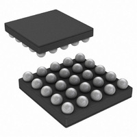
... Date Code. XYTT format. ‘XY’ 2 digit date code; ‘TT’ – dierun code — MNK - Package Marking — See National web page for more info - http://www.national.com/quality/marking_conventions.html Ordering Information Order Number Connector Debounce LP3918TL-L LP3918TLX-L LP3918TL-A LP3918TLX-A www.national.com LP3918 25 pin micro-SMD Package TOP VIEW 20211604 LDO MODE NO YES YES NO 2 ...
Page 3
LP3918 Pin Descriptions Pin # Name Type A1 IMON A A2 PS_HOLD DI A3 VSS G A4 RESET_N DO A5 ACOK_N DO B1 CHG_IN P B2 PWR_ON DI B3 SCL DI B4 PON_N DO B5 LDO7 A C1 BATT P ...
Page 4
Applications Schematic Diagram Device Description The LP3918 Charge Management and Regulator Unit is de- signed to supply charger and voltage output capabilities for mobile systems, e.g. CDMA handsets. The device provides a Li-Ion charging function and 7 regulated outputs. Communi- ...
Page 5
POWER SUPPLY CONFIGURATIONS At PMU start up, LDO1, LDO2 and LDO3 are always started with their default voltages. The start up sequence of the LDO's is given below. Startup Sequence LDO1 -> LDO2 -> LDO3 LDO's with external enable control ...
Page 6
... Absolute Maximum Ratings If Military/Aerospace specified devices are required, please contact the National Semiconductor Sales Office/ Distributors for availability and specifications. CHG-IN, VBATT =VIN1/2, BATT,HF_PWR All other Inputs Junction Temperature (T ) J-MAX Storage Temperature Max Continuous Power Dissipation (P ) (Note 3) D-MAX ESD (Note 4) Batt, VIN1, VIN2, HF_PWR, ...
Page 7
Symbol Parameter LOGIC AND CONTROL INPUTS (LDO2 at 3.0V) V Input Low Level IL V Input High Level IH I Logic Input Current IL R Input Resistance IN LOGIC AND CONTROL OUTPUTS (LDO2 at 3.0V) V Output Low Level OL ...
Page 8
LDO2 (DIGI) Electrical Characteristics Unless otherwise noted VIN1 = VIN2 = BATT) = 3.6V, GND = 0V 3. 0.5V. Typical values and limits appearing in normal type apply for T OUT2 apply ...
Page 9
LDO5 (RX), LDO6 (TX), LDO7 (GP) Electrical Characteristics Unless otherwise noted VIN1 = VIN2 = BATT) = 3.6V, GND = 0V Enabled via Serial Interface. Note V INMIN type apply for T = 25°C. Limits ...
Page 10
Charger Electrical Characteristics Unless otherwise noted 5V, V CHG-IN settings unless otherwise noted. Typical values and limits appearing in normal type apply for T boldface type apply over the entire junction temperature range for operation, T Symbol Parameter ...
Page 11
Serial Interface Unless otherwise noted VIN1 = VIN2 = BATT) = 3.6V, GND = 0V Typical values and limits appearing in normal type apply for T junction temperature range for operation, T Symbol Parameter f ...
Page 12
Register Information, Slave Address Code 7h’7E Register Addr D7 (default value) OP_EN 8h'00 X (0000 0101) LDO1PGM O/P 8h'01 X (0000 0001) LDO2PGM O/P 8h'02 X (0000 1011) LDO3PGM O/P 8h'03 X (0000 1011) LDO4PGM O/P 8h'04 X (0000 1011) ...
Page 13
LDO Output Voltage Programming The following table summarizes the supported output voltages for the LP3918. Default voltages after startup are highlighted in bold. Data Code LDO1 LDO2 (Reg 01 - 07) V 8h'00 1.5 8h'01 1.8 8h'02 1.85 8h'03 2.5 ...
Page 14
Charger Control Register 3 CHARGER TERMINATION VOLTAGE PROGRAMMING TABLE 6. LP3918 Charger Termination Voltage Control Address Register ID 8h'12 CHGCNTL3 END OF CHARGE CURRENT PROGRAMMING Address Register ID 8h'12 CHGCNTL3 CHARGING RESTART VOLTAGE PROGRAMMING Address Register ID 8h'12 CHGCNTL3 Charger ...
Page 15
Device Power Up and Shutdown Timing Device Power Up Logic Timing. PWR_ON 15 20211637 www.national.com ...
Page 16
Device Power Up Logic Timing. CHG_IN, HF_PWR 16 20211607 ...
Page 17
LP3918 Power On Behaviour (Failed PS_Hold) LP3918 Normal Shutdown Behaviour 17 20211608 20211633 www.national.com ...
Page 18
Functional Block Diagram www.national.com LP3918 Functional Block Diagram 18 20211602 ...
Page 19
Technical Description BATTERY CHARGE MANAGEMENT A charge management system allowing the safe charge and maintenance of a Li-Ion battery is implemented on the LP3918. This has a CC/CV linear charge capability with pro- grammable battery regulation voltage and end of ...
Page 20
CHARGER FULL RATE CURRENT Programming Information TABLE 12. Register Address 8h'11: CHGCNTL2 Data BITs HEX NAME 000[00000] 00 Prog_ICHG 000[00001] 01 000[00010] 02 000[00011] 03 000[00100] 04 000[00101] 05 000[00110] 06 000[00111] 07 000[01000] 08 000[01001] 09 000[01010] 0A 000[01011] ...
Page 21
Charger Operation The operation of the charger with EOC enabled is shown in this simplified flow diagram. FIGURE 2. Simplified Charger Functional Flow Diagram (EOC is enabled) 20211636 21 www.national.com ...
Page 22
The charger operation may be depicted by the following graphical representation of the voltage and current profiles. Further Charger Register Information Charger Control Register 1 TABLE 15. Register Address 8h'10: CHGCNTL1 BIT NAME FUNCTION (if bit = '1') 7 USB_MODE ...
Page 23
IMON CHARGE CURRENT MONITOR Charge current is monitored within the charger section and a proportional voltage representation of the charge current is presented at the IMON output pin. The output voltage rela- tionship to the actual charge current is represented ...
Page 24
INPUT CAPACITOR Input capacitors are required for correct operation rec- ommended that a 10µF capacitor be connected between each of the voltage input pins and ground (this capacitance value may be increased without limit). This capacitor must be ...
Page 25
No-Load Stability The LDO's on the LP3918 will remain stable in regulation with no external load. TABLE 20. LDO Output Capacitors Recommended Specification Symbol Parameter C Capacitance o(LDO1) C Capacitance o(LDO2) C Capacitance o(LDO3) C Capacitance o(LDO4) C Capacitance o(LDO5) ...
Page 26
FIGURE 6. Bit Transfer Each data transaction is composed of a Start Condition, a number of byte transfers (set by the software) and a Stop Condition to terminate the transaction. Every byte written to the SDA bus must be 8 ...
Page 27
CONTROL REGISTER WRITE CYCLE • Master device generates start condition. • Master device sends slave address (7 bits) and the data direction bit (r/w = “0”). • Slave device sends acknowledge signal if the slave address is correct. • Master ...
Page 28
FIGURE 10. Register Read Format 28 20211630 ...
Page 29
Physical Dimensions inches (millimeters) unless otherwise noted Thin micro-SMD25 Package NS Package Number MKT-TLA2511A X1 = 2.465mm ± 0.030mm X2 = 2.465mm ± 0.030mm X3 = 0.600mm ± 0.075mm 29 www.national.com ...
Page 30
... For more National Semiconductor product information and proven design tools, visit the following Web sites at: Products Amplifiers www.national.com/amplifiers Audio www.national.com/audio Clock and Timing www.national.com/timing Data Converters www.national.com/adc Interface www.national.com/interface LVDS www.national.com/lvds Power Management www.national.com/power Switching Regulators www.national.com/switchers LDOs www.national.com/ldo LED Lighting www ...