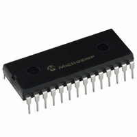
TC835CPI Microchip Technology, TC835CPI Datasheet - Page 6

TC835CPI
Manufacturer Part Number
TC835CPI
Description
IC ADC 4 1/2DGT BCD 28-DIP
Manufacturer
Microchip Technology
Datasheet
1.TC835CKW.pdf
(26 pages)
Specifications of TC835CPI
Display Type
LED
Configuration
7 Segment
Interface
BCD
Digits Or Characters
A/D 4.5 Digits
Current - Supply
1mA
Voltage - Supply
4 V ~ 6 V
Operating Temperature
0°C ~ 70°C
Mounting Type
Through Hole
Package / Case
28-DIP (0.600", 15.24mm)
Lead Free Status / RoHS Status
Lead free / RoHS Compliant
Available stocks
Company
Part Number
Manufacturer
Quantity
Price
Company:
Part Number:
TC835CPI
Manufacturer:
ST
Quantity:
6 217
TC835
3.0
(All Pin Designations Refer to 28-Pin DIP)
3.1
The TC835 is a dual slope, integrating analog-to-digital
converter. An understanding of the dual slope
conversion technique will aid in following the detailed
TC835 operational theory.
The conventional dual slope converter measurement
cycle has two distinct phases:
1.
2.
The input signal being converted is integrated for a
fixed time period, with time being measured by
counting clock pulses. An opposite polarity constant
reference voltage is then integrated until the integrator
output voltage returns to zero. The reference
integration time is directly proportional to the input
signal.
In a simple dual slope converter, a complete
conversion requires the integrator output to "ramp-up"
and "ramp-down."
A simple mathematical equation relates the input sig-
nal, reference voltage and integration time:
EQUATION 3-1:
For a constant V
EQUATION 3-1:
The dual slope converter accuracy is unrelated to the
integrating resistor and capacitor values, as long as
they are stable during a measurement cycle. An
inherent benefit is noise immunity. Noise spikes are
integrated, or averaged, to zero during the integration
periods. Integrating ADCs are immune to the large
conversion errors that plague successive approxima-
tion converters in high noise environments (see
Figure
DS21478C-page 6
Where:
T
DEINT
V
Input signal integration.
Reference voltage integration (de-integration).
T
REF
INT
3-1).
----------------------- -
R
INT
DETAILED DESCRIPTION
Dual Slope Conversion Principles
1
C
INT
=
=
=
IN
∫
V
T
0
:
INT
IN
Reference voltage
Reference voltage integration
time (variable)
Signal integration time (fixed)
V
=
IN
V
------------------------------- -
T ( )DT
REF
t
INT
T
DEINT
=
V
------------------------------- -
REF
R
INT
T
C
DEINT
INT
FIGURE 3-1:
3.2
The TC835 incorporates a system zero phase and
integrator output voltage zero phase to the normal two
phase dual slope measurement cycle. Reduced
system errors, fewer calibration steps and a shorter
overrange recovery time result.
The TC835 measurement cycle contains four phases:
1.
2.
3.
4.
Internal analog gate status for each phase is shown in
Table
3.2.1
During this phase, errors due to buffer, integrator and
comparator offset voltages are compensated for by
charging C
ing error voltage. With a zero input voltage the
integrator output will remain at zero.
The external input signal is disconnected from the
internal circuitry by opening the two SW
internal input points connect to ANALOG COMMON.
The reference capacitor charges to the reference
voltage potential through SW
closed around the integrator and comparator, charges
the C
buffer amplifier, integrator and comparator offset
voltages (see
Analog Input
Signal
Voltage
System zero.
Analog input signal integration.
Reference voltage integration.
Integrator output zero.
REF
Integrate
AZ
3-6.
Signal
Fixed
Time
Operational Theory
capacitor with a voltage to compensate for
AZ
SYSTEM ZERO
Polarity Control
(auto zero capacitor) with a compensat-
Figure
Variable
Reference
Integrate
Time
Display
Switch
Drive
Integrator
3-2).
-
+
Basic Dual Slope Converter.
© 2007 Microchip Technology Inc.
V
V
IN
IN
Control
Phase
≈
≈
V
1/2 V
REF
R
+
-
. A feedback loop,
Comparator
REF
Control
Logic
I
switches. The
Counter
Clock


