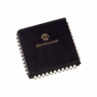
TC7126ACLW713 Microchip Technology, TC7126ACLW713 Datasheet - Page 10

TC7126ACLW713
Manufacturer Part Number
TC7126ACLW713
Description
IC ADC 3 1/2DGT LCD DVR 44-PLCC
Manufacturer
Microchip Technology
Datasheet
1.TC7126CPL.pdf
(26 pages)
Specifications of TC7126ACLW713
Display Type
LCD
Configuration
7 Segment
Digits Or Characters
A/D 3.5 Digits
Current - Supply
55µA
Voltage - Supply
9V
Operating Temperature
0°C ~ 70°C
Mounting Type
Surface Mount
Package / Case
44-PLCC
Lead Free Status / RoHS Status
Request inventory verification / Request inventory verification
Interface
-
Available stocks
Company
Part Number
Manufacturer
Quantity
Price
Company:
Part Number:
TC7126ACLW713
Manufacturer:
Microchip Technology
Quantity:
10 000
TC7126/A
4.0
In addition to the basic integrate and de-integrate dual
slope cycles discussed above, the TC7126A design
incorporates an auto-zero cycle. This cycle removes
buffer amplifier, integrator and comparator offset volt-
age error terms from the conversion. A true digital zero
reading results without external adjusting potentiome-
ters. A complete conversion consists of three phases:
1.
2.
3.
4.1
During the auto-zero phase, the differential input signal
is disconnected from the circuit by opening internal
analog gates. The internal nodes are shorted to analog
common (ground) to establish a zero input condition.
Additional analog gates close a feedback loop around
the integrator and comparator. This loop permits com-
parator offset voltage error compensation. The voltage
level established on C
voltages. The auto-zero phase residual is typically
10μV to 15μV. The auto-zero cycle length is 1000 to
3000 clock periods.
4.2
The auto-zero loop is entered and the internal differen-
tial inputs connect to V
input signal is integrated for a fixed time period. The
TC7126/A signal integration period is 1000 clock
periods or counts. The externally set clock frequency is
divided by four before clocking the internal counters.
The integration time period is:
EQUATION 4-1:
DS21458C-page 10
Where: F
Auto-Zero phase
Signal Integrate phase
Reference Integrate phase
ANALOG SECTION
Auto-Zero Phase
Signal Integrate Phase
OSC
T
= external clock frequency.
SI
=
AZ
F
IN
compensates for device offset
OSC
4
+ and V
x 1000
IN
-. The differential
The differential input voltage must be within the device
Common mode range when the converter and mea-
sured system share the same power supply common
(ground). If the converter and measured system do not
share the same power supply common, V
tied to analog common.
Polarity is determined at the end of signal integrate
phase. The sign bit is a true polarity indication, in that
signals less than 1LSB are correctly determined. This
allows precision null detection limited only by device
noise and auto-zero residual offsets.
4.3
The third phase is reference integrate or de-integrate.
V
V
ence capacitor. Circuitry within the chip ensures that
the capacitor will be connected with the correct polarity
to cause the integrator output to return to zero. The
time required for the output to return to zero is propor-
tional to the input signal and is between 0 and 2000
counts. The digital reading displayed is:
EQUATION 4-2:
IN
IN
- is internally connected to analog common and
+ is connected across the previously charged refer-
Reference Integrate Phase
1000
© 2006 Microchip Technology Inc.
V
V
REF
IN
IN
- should be


