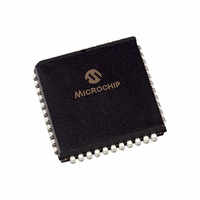
TC7126ACLW713 Microchip Technology, TC7126ACLW713 Datasheet - Page 12

TC7126ACLW713
Manufacturer Part Number
TC7126ACLW713
Description
IC ADC 3 1/2DGT LCD DVR 44-PLCC
Manufacturer
Microchip Technology
Datasheet
1.TC7126CPL.pdf
(26 pages)
Specifications of TC7126ACLW713
Display Type
LCD
Configuration
7 Segment
Digits Or Characters
A/D 3.5 Digits
Current - Supply
55µA
Voltage - Supply
9V
Operating Temperature
0°C ~ 70°C
Mounting Type
Surface Mount
Package / Case
44-PLCC
Lead Free Status / RoHS Status
Request inventory verification / Request inventory verification
Interface
-
Available stocks
Company
Part Number
Manufacturer
Quantity
Price
Company:
Part Number:
TC7126ACLW713
Manufacturer:
Microchip Technology
Quantity:
10 000
TC7126/A
6.0
6.1
The C
noise. A 0.47μF capacitor is recommended for 200mV
full scale applications where 1LSB is 100μV. A 0.033μF
capacitor is adequate for 2.0V full scale applications. A
mylar type dielectric capacitor is adequate.
6.2
The reference voltage, used to ramp the integrator out-
put voltage back to zero during the reference integrate
phase, is stored on C
able when V
Common mode voltage exists (V
mon) and the application requires a 200mV full scale,
increase C
than 0.5 count. A Mylar type dielectric capacitor is
adequate.
6.3
C
voltage swing without causing output saturation. Due to
the TC7126A’s superior analog common temperature
coefficient specification, analog common will normally
supply the differential voltage reference. For this case,
a ±2V full scale integrator output swing is satisfactory.
For 3 readings per second (F
value is suggested. For 1 reading per second, 0.15μF
is recommended. If a different oscillator frequency is
used, C
maintain the nominal ±2V integrator swing.
An exact expression for C
EQUATION 6-1:
At 3 readings per second, a 750Ω resistor should be
placed in series with C
compensating for comparator delay. C
low dielectric absorption to minimize rollover error. A
polypropylene capacitor is recommended.
DS21458C-page 12
Where:
INT
should be selected to maximize integrator output
F
V
R
V
AZ
OSC
FS
INT
INT
INT
COMPONENT VALUE
SELECTION
Auto-Zero Capacitor (C
Reference Voltage Capacitor (C
Integrating Capacitor (C
capacitor size has some influence on system
REF
= Clock frequency at Pin 38
= Full scale input voltage
= Integrating resistor
= Desired full scale integrator output swing
must be changed in inverse proportion to
REF
C
INT
to 1μF. Rollover error will be held to less
- is tied to analog common. If a large
=
(4000)
REF
INT
. A 0.1μF capacitor is accept-
. This increases accuracy by
INT
⎛
⎝
F
OSC
is:
V
OSC
1
INT
= 48kHz), a 0.047μF
REF
⎞
⎠
⎛
⎝
R
V
- – analog com-
INT
FS
AZ
INT
INT
⎞
⎠
)
must have
)
REF
)
6.4
The input buffer amplifier and integrator are designed
with Class A output stages. The output stage idling
current is 6μA. The integrator and buffer can supply
1μA drive current with negligible linearity errors. R
chosen to remain in the output stage linear drive
region, but not so large that PC board leakage currents
induce errors. For a 200mV full scale, R
2V full scale requires 1.8MΩ
6.5
C
equation:
EQUATION 6-2:
For a 48kHz clock (3 conversions per second),
R = 180kΩ.
Note that F
internal clock. The backplane drive signal is derived by
dividing F
To achieve maximum rejection of 60Hz noise pickup,
the signal integrate period should be a multiple of
60Hz. Oscillator frequencies of 24kHz, 12kHz, 80kHz,
60kHz, 40kHz, etc. should be selected. For 50Hz rejec-
tion,
66-2/3kHz, 50kHz, 40kHz, etc. would be suitable. Note
that 40kHz (2.5 readings per second) will reject both
50Hz and 60Hz.
C
R
C
Component
OSC
Note:
AZ
INT
INT
Value
oscillator
should be 50pF; R
Integrating Resistor (R
Oscillator Components
OSC
F
OSC
OSC
by 800.
frequencies
is 44 to generate the TC7126A’s
= 48kHz (3 readings per sec).
Nominal Full Scale Voltage
0.047μF
F
200mV
0.33μF
180kΩ
OSC
© 2006 Microchip Technology Inc.
=
OSC
.
0.45
RC
of
is selected from the
20kHz,
INT
INT
0.033μF
0.047μF
1.8MΩ
)
2V
is 180kΩ. A
100kHz,
INT
is


