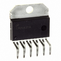
LM2463TA/NOPB National Semiconductor, LM2463TA/NOPB Datasheet - Page 6

LM2463TA/NOPB
Manufacturer Part Number
LM2463TA/NOPB
Description
IC DRIVER MONOLITHIC TO-220-11
Manufacturer
National Semiconductor
Datasheet
1.LM2463TANOPB.pdf
(12 pages)
Specifications of LM2463TA/NOPB
Display Type
CRT
Current - Supply
50mA
Voltage - Supply
60 V ~ 85 V
Operating Temperature
-20°C ~ 100°C
Mounting Type
Through Hole
Package / Case
TO-220-11 (Bent and Staggered Leads)
Lead Free Status / RoHS Status
Lead free / RoHS Compliant
Interface
-
Configuration
-
Digits Or Characters
-
Other names
*LM2463TA
*LM2463TA/NOPB
LM2463TA
LM2463TANOPB
LM2463TANOPB
*LM2463TA/NOPB
LM2463TA
LM2463TANOPB
LM2463TANOPB
www.national.com
Application Hints
OPTIMIZING TRANSIENT RESPONSE
Referring to Figure 9 , there are three components (R1, R2
and L1) that can be adjusted to optimize the transient re-
sponse of the application circuit. Increasing the values of R1
and R2 will slow the circuit down while decreasing over-
shoot. Increasing the value of L1 will speed up the circuit as
well as increase overshoot. It is very important to use induc-
tors with very high self-resonant frequencies, preferably
above 300 MHz. Ferrite core inductors from J.W. Miller
Magnetics (part # 78FR--k) were used for optimizing the
performance of the device in the NSC application board. The
values shown in Figure 10 and Figure 11 can be used as a
good starting point for the evaluation of the LM2463. Using a
variable resistor for R1 will simplify finding the value needed
for optimum performance in a given application. Once the
optimum value is determined, the variable resistor can be
replaced with a fixed value.
EFFECT OF LOAD CAPACITANCE
Figure 8 shows the effect of increased load capacitance on
the speed of the device. This demonstrates the importance
of knowing the load capacitance in the application.
EFFECT OF OFFSET
Figure 7 shows the variation in rise and fall times when the
output offset of the device is varied from 40 to 50 V
rise time shows a maximum variation relative to the center
data point (45 V
less than 6% relative to the center data point.
THERMAL CONSIDERATIONS
Figure 4 shows the performance of the LM2463 in the test
circuit shown in Figure 2 as a function of case temperature.
The figure shows that the rise and fall times of the LM2463
increase by approximately 10% as the case temperature
increases from 50˚C to 100˚C. This corresponds to a speed
degradation of 2% for every 10˚C rise in case temperature.
Figure 6 shows the maximum power dissipation of the
LM2463 vs. Frequency when all three channels of the device
are driving an 8 pF load with a 40 V
on, one pixel off signal. The graph assumes a 72% active
time (device operating at the specified frequency) which is
typical in a monitor application. The other 28% of the time
the device is assumed to be sitting at the black level (65V in
this case). This graph gives the designer the information
needed to determine the heat sink requirement for his appli-
cation. The designer should note that if the load capacitance
is increased the AC component of the total power dissipation
will also increase.
DC
FIGURE 9. One Channel of the LM2463 with the Recommended Arc Protection Circuit
) of 4%. The fall time shows a variation of
(Continued)
p-p
alternating one pixel
DC
. The
6
The LM2463 case temperature must be maintained below
100˚C. If the maximum expected ambient temperature is
70˚C and the maximum power dissipation is 11.9W (from
Figure 6 , 180 MHz bandwidth) then a maximum heat sink
thermal resistance can be calculated:
This example assumes a capacitive load of 8 pF and no
resistive load.
TYPICAL APPLICATION
A typical application of the LM2463 is shown in Figure 10
and Figure 11 . Used in conjunction with an LM1263, a com-
plete video channel from monitor input to CRT cathode can
be achieved. Performance is ideal for 1600 x 1200 resolution
displays with pixel clock frequencies up to 180 MHz. Figure
10 and Figure 11 are the schematic for the NSC demonstra-
tion board that can be used to evaluate the LM126X/2463
combination in a monitor.
PC BOARD LAYOUT CONSIDERATIONS
For optimum performance, an adequate ground plane, iso-
lation between channels, good supply bypassing and mini-
mizing unwanted feedback are necessary. Also, the length of
the signal traces from the preamplifier to the LM2463 and
from the LM2463 to the CRT cathode should be as short as
possible. The following references are recommended:
Ott, Henry W., “Noise Reduction Techniques in Electronic
Systems”, John Wiley & Sons, New York, 1976.
“Video Amplifier Design for Computer Monitors”, National
Semiconductor Application Note 1013.
Pease, Robert A., “Troubleshooting Analog Circuits”,
Butterworth-Heinemann, 1991.
Because of its high small signal bandwidth, the part may
oscillate in a monitor if feedback occurs around the video
channel through the chassis wiring. To prevent this, leads to
the video amplifier input circuit should be shielded, and input
circuit wiring should be spaced as far as possible from output
circuit wiring.
NSC DEMONSTRATION BOARD
Figure 12 shows the routing and component placement on
the NSC LM126X/2463 demonstration board. The schematic
of the board is shown in Figure 10 and Figure 11 . This board
DS200128-10


